An inside look: LCD and E-Ink displays
Demain n'existe pas!
In the last article in the series “A View from the Inside,” we talked about everyday things, but, despite the abundance of material received in this direction over the past month, let’s return to the topic related to IT.
')
Especially for the Day of Defender of the Fatherland, LCD and E-Ink displays lay on the preparatory table, which, one way or another, I got in a bit beaten form of life.
As Anton threw the phone against the wall, as well as the results of a rigorous analysis of the displays read under the cut.
Foreword
Once upon a time there lived Anton Gorodetsky.
He left his wife, he was sad not childish ...
So begins the famous song of the band Umaturman. The story begins with the study of displays. After the first publication on Habré, my friend, a graduate student of FNM MSU, came to me and said: “I broke my mobile phone here, would you like to saw it?” I was surprised because this person always carried with him a chitaphone, which I considered practically not kill Having come home one day, Anton, out of habit, threw the phone into the closet, but, apparently, without calculating something, it hit the display on the edge of the shelf.
Aware of his ridiculous losses from the loss of the mobile and in view of the general bad mood that day, he acted like a true gentleman, hurling the lifeless body of the phone over and over the concrete wall. When the remains reached me, then half of the chinophone was simply absent, the display was covered with a small spiderweb of cracks.
I had to postpone it until better times (as I then thought, until someone came in the same way with the iPhone or another touchscreen smartphone) and started working on HDD and CD, then light bulbs, flash drives, etc.
After a while, my neighbor already brings me a cracked E-Ink display. His friend broke a thin glass in the famous reading room with the serial number 601 during the game in airsoft, it seems, and gave the reader almost nothing for repair and restoration.
Now that was more interesting, the two technologies can be compared with each other, try to make out the RGB subpixels and the microcapsules in which charged particles float. But I was hoping to get a smartphone with a capacitive sensor in order to compare it at the same time with its resistive sensor of the Chinese phone.
And Vasily (a scientific colleague in one of the faculty's laboratories), coming to us at HimFak from Chernogolovka and seeing what I actually do with an electron microscope, said he was ready to sacrifice the phone of a famous Korean manufacturer with a slightly beaten display for disassembling and cutting with a mark "For the sake of science, nothing is pitiful."
Despite all the assurances that the sensor is capacitive, it turned out to be resistive, albeit a more advanced design, than the touch panel of a chinaphone. An important detail was extracted from this phone that is waiting to be cut in its time - a photo / video camera matrix ...
Part theoretical
How does the LCD display work?
We all have been using flat-screen TVs, monitors, telephones, smartphones for so long that we have already forgotten that a once-good monitor weighed 10-15 kilograms (we have one such mastodon still standing and, most importantly, it works fine!).
All this was made possible thanks to the discoveries of a century ago (liquid crystals were discovered in 1888) and the development of technology in the last 30-40 years (1968 - a device for displaying information using LCD, 1970s - the general availability of liquid crystals). Much about liquid crystals and LCD monitors can be found on the Wiki.
So, almost any LCD monitor consists of the following main parts: the active matrix, which is a set of transistors with which the image is formed, a layer of liquid crystals with light filters that either transmit light or not, and the backlight system, which today Try to fully translate to LEDs. Although on my “old” Asus G2S the display of superb quality is illuminated with fluorescent lamps.
How does all this work? Light coming from a source (LED or lamp) through a special transparent plate-waveguide is scattered so that the entire matrix has equal illumination over its entire area. Next, the photons pass through the polarization filter, which transmits only waves with a given polarization . Then, penetrating the glass substrate, on which the active matrix of thin-film transistors is located, light strikes the liquid crystal molecule.
This molecule receives a “command” from the underlying transistor, at what angle to rotate the polarization of the light wave, so that it, passing through another polarization filter, sets the intensity of the glow of a separate subpixel. And for the color subpixels responsible layer of light filters (red, green or blue). When mixing, the waves from three subpixels that are invisible to the human eye form a pixel of an image of a given color and intensity.
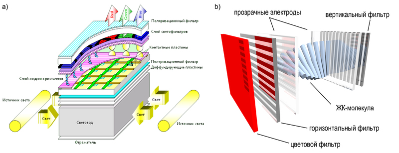
a) A schematic LCD display device, b) a liquid crystal film device in detail.
Very clearly, as it seems to me, this is demonstrated in the Sharp company video:
In addition to the well-proven LCD + TFT technology (thin-film transistors - thin-film transistors), there is an actively promoted technology of organic LEDs OLED + TFT, that is, AMOLED - active matrix OLED. The main difference of the latter lies in the fact that the role of a polarizer, a layer of LCDs and light filters is played by organic LEDs of three colors.
In essence, these are molecules capable of emitting light during the flow of electric current, and depending on the amount of current flowing, they change the color intensity, just as it happens in ordinary LEDs. By removing the polarizers and the LCD from the panel, we can potentially make it more subtle and, most importantly, flexible!
What touch panels are there?
Since the sensors are currently used more with LCD and OLED displays, I think it would be wise to talk about them right away.
A very detailed description of the tan screens or touch panels is given here (the source once lived here , but for some reason disappeared), so I will not describe all types of touch panels, I’ll dwell only on two main ones: resistive and capacitive.
Let's start with a resistive sensor. It consists of 4 main components: a glass panel (1), as a carrier of the entire touch panel, two transparent polymer membranes with a resistive coating (2, 4), a layer of microinsulators (3) separating these membranes, and 4, 5 or 8 wires, which are responsible for “reading” the touch.
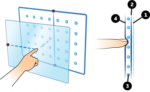
Diagram of the resistive sensor device
When we press on such a sensor with a certain force, the contact of the membranes occurs, the electrical circuit closes, as shown in the figure below, the resistance is measured, which is subsequently recalculated into coordinates:
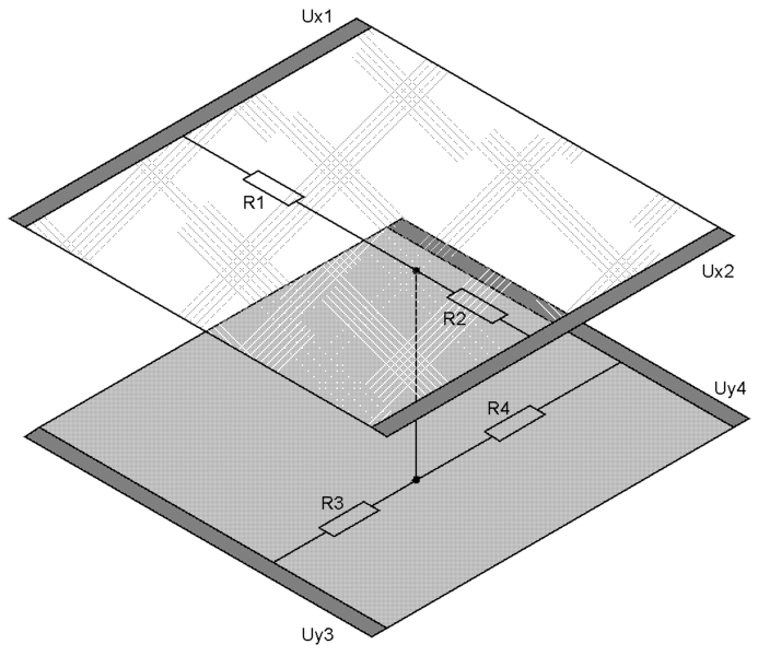
The principle of calculating the coordinates for a 4-wire resistive display ( Source )
Everything is very simple.
It is important to remember two things: a) resistive sensors on many Chinese phones are not of high quality, this may be due just to the uneven distance between the membranes or poor-quality micro-insulators, that is, the “brain” of the phone cannot adequately recalculate the measured resistances into coordinates; b) such a sensor requires precisely pressing, forcing one membrane to another.
Capacitive sensors are somewhat different from resistive. It should immediately make a reservation that we will talk only about the projection-capacitive sensors, which are now used in the iPhone and other portable devices.
The principle of operation of such a touchscreen is quite simple. On the inner side of the screen, a grid of electrodes is applied, while the outer one is covered, for example, ITO with a complex indium tin oxide. When we touch the glass, our finger forms a small capacitor with such an electrode, and the processing electronics measure the capacitance of this capacitor (it gives a current pulse and measures the voltage).
Accordingly, the capacitive sensor responds only to a dense touch and only with conducting objects, that is, if touched with a nail, such a screen will work every other time, as well as from a hand soaked in acetone or dehydrated. Perhaps the main advantage of this touchscreen over resistive is the ability to make a sufficiently strong base - extra strong glass, such as, for example, Gorilla Glass.

Scheme of operation of the surface-capacitive sensor ( Source )
How does the E-Ink display?
Perhaps, E-Ink is much easier compared to LCD. Again, we are dealing with an active matrix, which is responsible for image formation, however, LCD crystals and backlights are not mentioned here, instead of them there are cones with two types of particles: negatively charged black and positively charged white ones. The image is formed by applying a certain potential difference and the redistribution of particles inside such microcollows, in the figure below this is clearly demonstrated:

Top diagram of the E-Ink display, bottom real micrographs of such a working display ( Source )
If this is not enough for someone, the principle of the electronic paper is shown in this video:
In addition to the E-Ink technology, there is SiPix technology, in which there is only one kind of particles, and the “fill” itself is black:

SiPix display operation scheme ( Source )
Those who seriously want to get acquainted with the "magnetic" electronic paper, I ask you here , there was once a great article at Perst.
Part practical
Chinaphone vs Korean smartphone (resistive sensor)
After a “neat” screwdriver disassembly of the board and display left over from the phone box, I was surprised to find the mention of a famous Korean manufacturer on the phone’s motherboard:
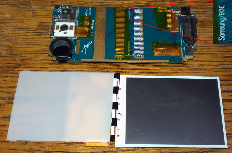
Samsung and ChinaPhone are one!
The screen was carefully and carefully disassembled - so that all the polarizers remained intact, so I just could not play with them and with the working big brother of the object being prepared and recall the optics workshop:

This is how 2 polarization filters work : in one position, the luminous flux practically does not pass through them, when rotated by 90 degrees - completely passes
Please note that all the lighting is based only on four tiny LEDs (I think their total power is not more than 1 W).
Then I searched the sensor for a long time, sincerely believing that it would be a rather thick socket. It turned out quite the opposite. In both Chinese and Korean phones, the sensor consists of several sheets of plastic that are very high quality and tightly glued to the glass of the outer panel:
On the left, the sensor of the cellphone, on the right - the Korean phone
The resistive sensor of the Chinese phone is made according to the scheme “the simpler the better”, unlike its more expensive fellow from South Korea. If I'm wrong, then correct me in the comments, but on the left in the picture is a typical 4-pin, and on the right is an 8-pin sensor.
LCD display
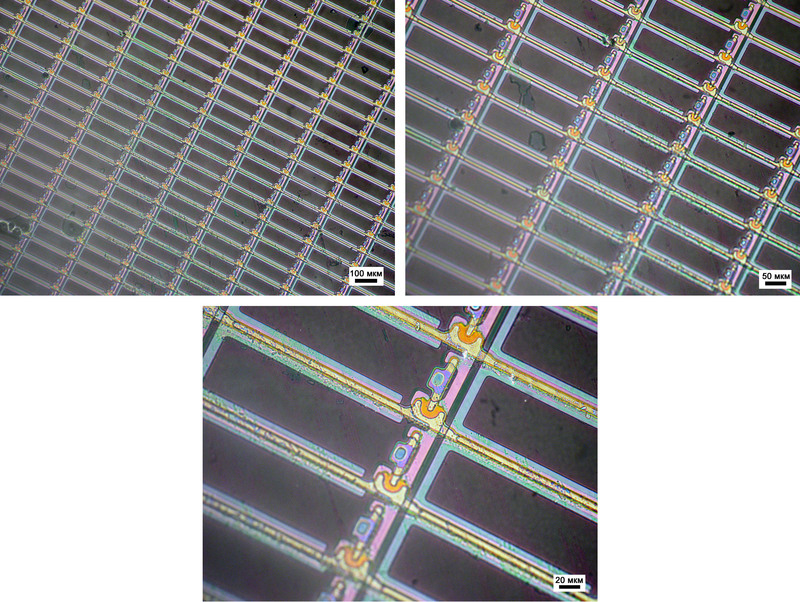
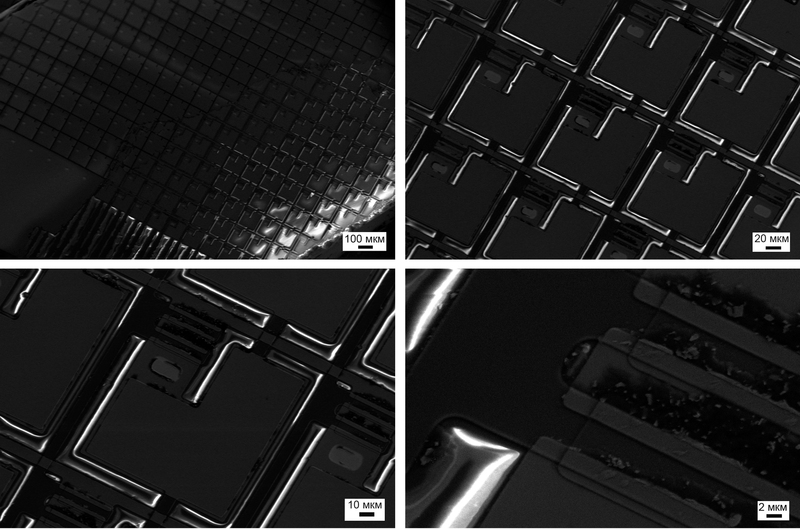
Since the display of the Chinese phone was still broken, and the Korean one was only slightly damaged, then using the example of the first one, I will try to tell about the LCD. But for now, we will not break it completely, but look under an optical microscope:

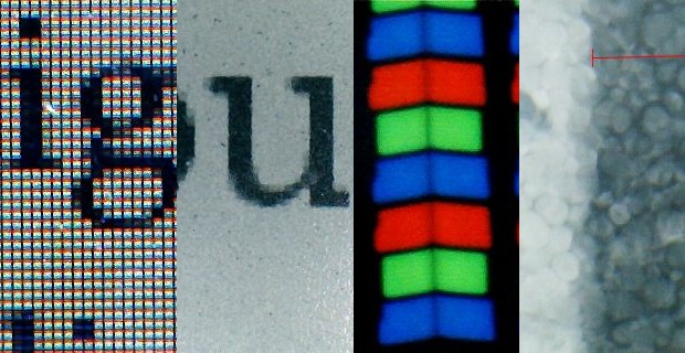
Optical micrograph of horizontal lines of the LCD of a Chinese phone. There is a certain deception of our view due to the “wrong” colors inherent in the top left photo: a white thin strip is a contact.
One wire feeds at once two lines of pixels, and the isolation between them is arranged with the help of a completely unusual “electric beetle” (lower right photo). Behind this circuitry, there are light paths painted in the corresponding colors: red (R), green (G) and blue (B).
From the opposite end of the matrix in relation to the place of attachment of the cable, you can find a similar color breakdown, track numbers and all the same switches (if someone had clarified in the comments how it works, then it would be great!):

Numbers Numbers Numbers ...
This is how a live LCD display looks like under a microscope:
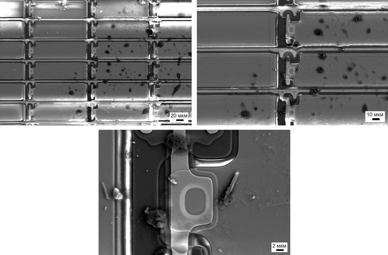
That's all, now we will not see this beauty, I crushed in the literal sense of the word, and having a little tortured one such crumb “split” into two separate pieces of glass, of which the main part of the display consists ...
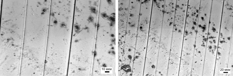
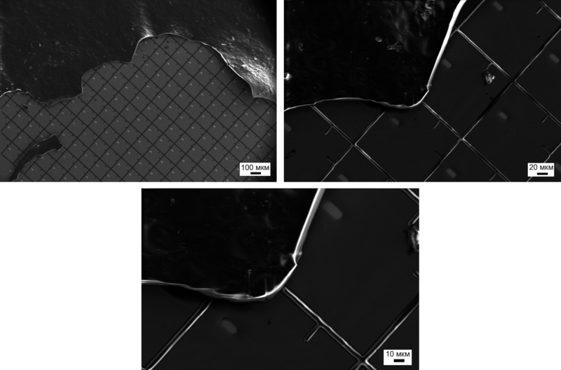
Now you can look at the individual lanes of filters. I will talk about dark "spots" on them a bit later:
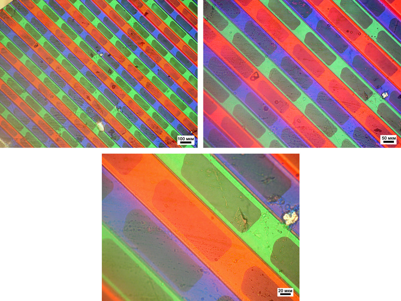
Optical micrograph of light filters with mysterious spots ...
And now a small methodological aspect concerning electron microscopy. The same color bands, but under the electron microscope beam: the color has disappeared! As I said earlier (for example, in the very first article ), the electron beam is completely “black and white” whether it interacts with a colored substance or not.
It seems to be the same stripes, but without the color ...
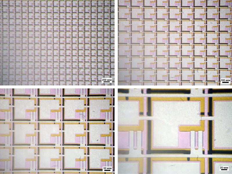
Look at the opposite side. It contains transistors:
In an optical microscope - in color ...
And the electron microscope is a black and white image!
In the optical microscope, this can be seen a little worse, but the EMS allows you to see the border of each subpixel - this is quite important for the following output.
So what are these strange dark areas ?! I thought for a long time, puzzled myself, read many sources (perhaps the Wiki was the most accessible) and, by the way, for this reason I delayed the release of the article on Thursday February 23. And so to what conclusion I came (perhaps I am not right - correct!).
VA or MVA technology is one of the simplest, and I don’t think that the Chinese came up with something new: each subpixel should be black. That is, light does not pass through it ( here is an example of a working and non-working display), taking into account that in the “normal” state (without the application of external influence) the liquid crystal is disoriented and does not give the “desired” polarization, it is logical to assume that Each individual subpixel has its own film with LCD.
Thus, the entire panel is assembled from single micro-LCD displays. The note about the fringing of each individual subpixel fits well here. For me, this was a kind of unexpected discovery right during the preparation of the article!
I regretted displaying a Korean phone: I need to show something to children and those who come to our faculty on a tour. I do not think that it would be possible to see something else interesting.
Further, for the sake of pampering, I will give an example of the "organization" of pixels from the two leading communicator manufacturers: HTC and Apple. iPhone 3 was donated for a painless operation by one kind person, and HTC Desire HD is actually mine:

Micrograph of the display HTC Desire HD
A small note about the HTC display: I did not specifically look for it, but could this strip in the middle of the top two micrographs be that part of that very capacitive sensor ?!

Photomicrographs of the iPhone 3 display
If my memory serves me, the HTC display has a superLCD, and the iPhone 3 has a regular LCD. The so-called Retina Display, that is, LCD, in which both contacts for switching liquid crystal lie in the same plane, In-Plane Switching - IPS, is already installed in the iPhone 4.
I hope that soon an article with the support of 3DNews will be released on the topic of comparing different display technologies. In the meantime, I just want to note the fact that the HTC display is really unusual: contacts on separate subpixels are made in a non-standard way - somehow from above, unlike the iPhone 3.
And finally, in this section, I’ll add that the size of one subpixel for a Chinese phone is 50 by 200 micrometers, HTC is 25 by 100 micrometers, and the iPhone is 15-20 by 70 micrometers.
E-Ink famous Ukrainian manufacturer
Let's start with the commonplace things - "pixels", or rather the cells that are responsible for the formation of the image:
Optical micrograph of the active matrix of the E-Ink display
The size of such a cell is about 125 micrometers. Since we are looking at the matrix through the glass on which it is applied, I ask you to pay attention to the yellow layer in the “background” - this is a gold plating, which we will later have to get rid of.
Next, the current-carrying contacts. This photo especially impressed me:
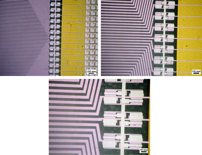
Next to the embrasure!

Comparison of horizontal (left) and vertical (right) "inputs"
Among other things, a lot of interesting things were found on the glass substrate. For example, positional labels and contacts, which, apparently, are intended to test the display in production:

Optical micrographs of tags and test pads
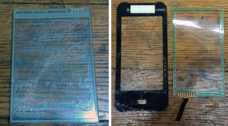
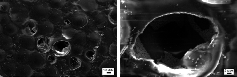
Of course, this does not happen often and is usually an accident, but the displays sometimes break. For example, this barely noticeable crack with a thickness less than a human hair can forever deprive joy of reading a favorite book about Albion in a stuffy Moscow metro:

If the displays break, then it needs someone ... I, for example!
By the way, here it is, the gold I mentioned - a smooth pad “from the bottom” of the cell for high-quality contact with the ink (about them just below). Gold is removed mechanically and the result is:
You've got a lot of guts. Let's see what they look like! (with)
The control components of the active matrix are hidden under a thin gold film, if you can call it that.
But the most interesting, of course, is the ink itself:
SEM micrograph of ink on the active matrix surface.
Of course, it is difficult to find at least one broken microcapsule to look inside and see the “white” and “black” pigment particles:
SEM micrograph of electronic ink surface
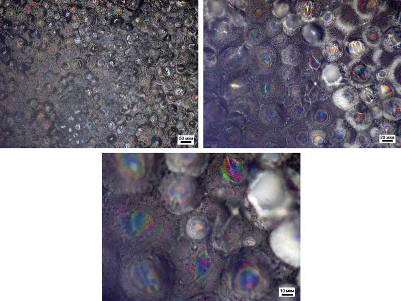
Optical micrograph of "ink"
Or is there something inside?
Whether the destroyed sphere, or torn from the carrier polymer
The size of individual balls, that is, some analogue of a sub-pixel in an E-Ink, can be as low as 20-30 μm, which is significantly lower than the geometric dimensions of sub-pixels in LCD displays. Provided that such a capsule can work in half its size, then the image obtained on a good, high-quality E-Ink displays is much more pleasant than on the LCD.
And for dessert - a video about how E-Ink displays work under a microscope:
Conclusion
At the end of my story, I would like to thank those who helped me in writing this article: Anton (the broken sieve of his hands), Alexei (the injured E-Ink, who was torn out of the tenacious paws of the service), Basil (for the Korean phone, camera which will be the hero of one of the following publications), Masha (who was not afraid to give me her iPhone), Katerina (for justifying her last name).
PS In the end, the account managed to snatch a small piece of the reader and study the technology of flexible electronics promoted by RosNano .
First , the full list of published articles on Habré:
Opening the Nvidia 8600M GT chip , a more detailed article is given here: Modern chips - a view from the inside
An inside look: CD and HDD
An inside look: LED bulbs
An inside look: the LED industry in Russia
An inside look: Flash and RAM
An inside view: the world around us
An inside look: LCD and E-Ink displays
An inside look: matrix digital cameras
An inside look: Plastic Logic
An inside look: RFID and other tags
An inside look: graduate school at EPFL. Part 1
An inside look: graduate school at EPFL. Part 2
An inside view: the world around us - 2
An inside view: the world around us - 3
An inside look: the world around us - 4
An inside look: 13 LED lamps and a bottle of rum. Part 1
An inside look: 13 LED lamps and a bottle of rum. Part 2
An inside look: 13 LED lamps and a bottle of rum. Part 3
An inside look: IKEA LED strikes back
An inside view: are Filament lamps good for you?
and 3DNews:
Microview: a comparison of modern smartphones displays
Secondly , in addition to the blog on HabraHabr , articles and videos can be read and viewed on Nanometer.ru , YouTube , and Dirty .
Thirdly , if you, dear reader, liked the article or you want to stimulate writing new ones, then act according to the following maxim: “pay what you want”
Yandex.Money 41001234893231
WebMoney (R296920395341 or Z333281944680)
Sometimes briefly, and sometimes not so much about the news of science and technology, you can read on my Telegram channel - welcome;)
Source: https://habr.com/ru/post/138833/
All Articles