Designing synchronous circuits. Quick Start with Verilog HDL
 On the Internet, you can find quite a few articles with an introduction to Verilog HDL. All of them describe the syntax and semantics of the language, but, unfortunately, do not reveal the main paradigms used in the design of digital circuits. Imagine that the syntax of the Java language is explained to you, but they do not tell you anything about object-oriented design. If you are familiar with OOP, then such an introduction will be enough, but if you know only C, then you will most likely write “as before”, creating huge classes with complex methods.
Something like this happens to programmers who study digital circuitry and hardware description languages. Having quickly dealt with the simple syntax of the language, they begin to describe constructs that are insane from the point of view of the hardware engineer. Among my students there were people who wrote “bubble sorting” per clock, crazy asynchronous circuits that worked differently with each launch and different weather outside the window, huge combinational dividers that took place & route into deep hours of thoughtfulness.
For those who do not have time to read a primer, but there is a desire or
the need to design some simple circuits I decided to write this small introduction about the main modern paradigm of digital circuit design - synchronous circuits. And about one of the languages used to describe them.
The article is designed for beginners. To understand the text will require a minimum set of knowledge - an understanding of the synchronous D-trigger and valves.
Synchronous circuits
Synchronous digital circuits consist of combinational valves (gates), circuits (nets) and flip-flops. In the synchronous scheme there is a single synchronization signal that controls all the memory elements (triggers).
')
Formally, the synchronous scheme can be defined as follows:
A synchronous circuit is a digital circuit C consisting of gates, triggers and signal propagation circuits that satisfies the following conditions:
- There is a single clk circuit in the circuit through which the synchronization signal (clock signal, clock signal) is distributed.
- The clk signal is controlled by the input port of the circuit.
- The set of ports controlled by the clk signal is equivalent to the set of trigger trigger inputs
- We define circuit C ' as follows: Circuit C' is obtained from circuit C by: (1) removing the clk circuit, (2) removing the input port that controls the signal clk , (3) replacing all the triggers with the output port (instead of input D) and the input port (instead of output Q). The resulting scheme C ' must be a combination
An example of a synchronous circuit is shown in the figure:
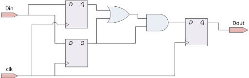
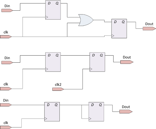
Here are some examples of non-synchronous circuits:
Almost all existing digital circuits are synchronous, or consist of several synchronous circuits that interact through asynchronous channels. The reason for the popularity of synchronous circuits is in the simplicity of analyzing the propagation time of signals. Timing analysis is a topic for a separate article, but we need to briefly touch upon this issue.
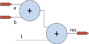
Consider the following scheme that implements the function R = A + B + 1:
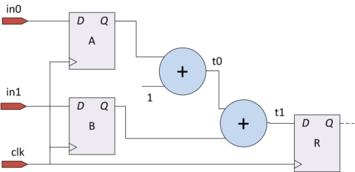
Registers A, B and R store the values at the inputs D on the leading edge of the synchronization signal (clk), i.e. at that point in time when the value of clk changes from 0 to 1.
Signals propagate through adders (and other combinational elements) not instantaneously, but with a delay depending on the length of the longest path from the gates (the critical path), i.e. on the complexity of the item. For example, the critical path in the adder will pass through the transfer signals to the high bit (imagine the calculation of the sum by the “bar”).
Suppose that first in all registers was written 0. And the inputs in0, in1 first served the values 1 and 4, and then 2 and 1. Then the timing diagram for our circuit might look like this:
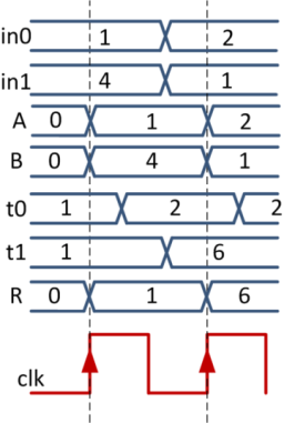
On the first edge of clk, the values 1 and 4 will be written to registers A and B. After the signal propagates through the adders, the result value 1 + 4 + 1 = 6 appears on the wire t1. Then, on the second front clk, the result will be written to register R, and the new input values to registers A and B.
Now imagine that the period of the signal clk is halved. Then the second edge of the clk signal appears on the register R before the correct data appears on t1. Those. The circuit will not work correctly!
From here follows the basic rule for the correct operation of a synchronous scheme:
The delay through the critical path in the circuit must be less than the period of the synchronization signal.
The critical path is the longest path in the circuit, from the output to the register entry. From this rule, a consequence is derived that characterizes one of the biggest drawbacks of synchronous schemes:
The synchronous circuit operates at a frequency determined by the critical path in the circuit.
Imagine that in the scheme there are thousands of combinational paths with a delay of 1 nanosecond. And one way with a delay of 2 nanoseconds. Because of this single path, the circuit must be clocked at a frequency of 500 MHz, although it could operate at a gigahertz. Therefore, when designing synchronous circuits, long combination chains are divided by registers into conveyor stages. For example, in the AMD Bulldozer processor, the average length of the combinational path is 12-14 FO4 equivalent gates (the delay is equivalent to a unit-sized inverter loaded with 4 inverters).
Despite this drawback, synchronous circuits have become very popular. Synchronous circuits can easily be automatically timed analyzed, i.e. The frequency at which the circuit can work correctly is automatically determined by the program (time analyzer). When a developer can move away from these details, the synchronous scheme can be specified by a set of transfers between registers. This approach to the description of the schemes - Register Transfer Logic (RTL) has become the mainstream in the description of the logic of the digital circuits. For example, the scheme from our example can be described with the following shipments:
A = in0
B = in1
R = A+B+1
At each cycle, in0 is written in register A, in1 is written into register B, and A + B + 1 is written into register R. The idea to describe the schemes in RTL as text is the basis of the hardware description languages: Verilog HLD and VHDL. It's time to get to know one of them.
Description of synchronous circuits on Verilog HDL
Modules
The program on Verilog, which is also a description of the scheme, consists of modules (module), more precisely, module instances of modules. The module can be represented as a “black box” with wires sticking out of it - ports (ports). Ports are of three types: input (input), output (output) and bidirectional (inout). In most cases, the first two types of ports are used. Bidirectional ports are needed to simulate bidirectional tires, based on tri-state outputs and open drain. We will not consider them.
The list of ports is described in the module header. For example, consider this empty module:
module blackbox // module - , blackbox -
(
input a, b, c // a,b,c
input [7:0] bus, // bus - 8-
output [7:0] bus_out // bus_out, 8-
);
//

endmodule // endmodule - ,
The module body describes its functionality. This module is empty, its ports are not connected anywhere. Before proceeding to the description of the functionality of the modules, let's get acquainted with the main data types in Verilog.
Data types
There are two types of classes in Verilog: hardware modeling types and standard arithmetic data types copied from C language. We will consider only the first of the classes, because it is used to model the signals in the circuit.
In Verilog, the signal can take 4 values:
- 0 - logical zero, or false
- 1 - logical unit, or true
- x is an undefined value. For example, the value of the register at the initial moment of the simulation (before the reset or the first entry in the register)
- z is a state with high impedance. Most often the signal takes this value if it is not connected anywhere - “wire break”
Most modules on Verilog use 2 basic data types - wire and reg . From the name it may seem that wire simulates a wire, and reg - a register, but, as will be shown later, this is not quite so. The presence of two types is rather a bug in the design of the language; in SystemVerilog, the modern version of Verilog, there is a universal type of logic that can be used in all cases.
Consider each of the types separately.
Wires
The wire type is used to simulate signals that cannot “store” a state. For example, the value at the output of the combinator circuit is completely determined by the values at the inputs. If the input values change, the output value also changes, i.e. state is not stored. The wire type is used in conjunction with the continuous assignment operation, assign . With continuous assignment, whenever the value of the variables on the right side of the assignment changes, the value of the variable on the left side is updated. For example, a simple combinational circuit can be described as follows:
module comb
(
input wire [7:0] a,b,
output [7:0] res // wire -, output wire [7:0] res
);

assign res = a+b+1;
endmodule
Signals can also be declared inside the module body:
module comb
(
input wire [7:0] a,b,
output [7:0] res
);

wire [3:0] x,y;
assign x = a[3:0] + b[3:0]; // 4 b
assign y = a[7:4] + b[7:4]; // 4 b
assign res = x+y;
endmodule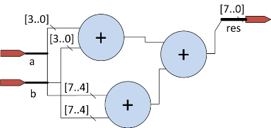
Regs
The reg type can hold a value and is used in procedural blocks. A procedural block in Verilog is a routine triggered by a specific event. For example, this event may be the front of a clock signal or the start of a simulation. In procedural blocks, C-like control structures can be used:
- if ... else ..
- for
- do ... while ..
- case (analog switch)
Procedural blocks can simulate both synchronous circuits (circuits with memory) and combinational circuits. For example, consider the description of a binary counter scheme:
module counter
(
input clk, reset,
output [7:0] data
);
reg [7:0] counter;

assign data = counter;

always @( posedge clk) // clk
begin
if (reset)
counter = 0;
else
counter = counter + 1;
end

endmodule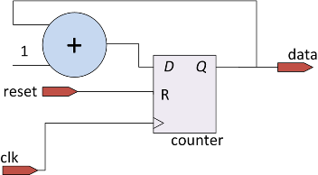
The string always @ ( posedge clk) is called the sensitivity list. It defines the events on which the procedural block is executed. This block is performed on each positive edge of the synchronization signal. Thus, the block simulates the logic of the counter, the signal counter will be synthesized as a register.
Procedural blocks can simulate and combinational schemes. For example, the following code is synthesized into a combinational adder:
wire [7:0] a,b;
reg [7:0] res;

always @*
begin
res = a+b;
end
Here, the always @ * sensitivity list means that the procedural block is executed each time the values of the signals in the right-hand part of the assignment change. In this case, the procedural block is triggered every time the signals a and b change. Equivalent to this line will be the following list of sensitivity:
always @(a or b) // , a b
When describing the combinational circuit with the help of the procedural block always it is necessary to remember that the values of all the signals changing in the block must be completely determined by the signals in the sensitivity list. Otherwise, the synthesizer will have to insert into the circuit the elements of memory - latches (latches).
For example, consider the following procedural block:
wire a,b;
reg res;

always @*
begin
if(a & b) res = 1;
else if (!a & b) res = 0;
end
The procedural block does not describe what will happen if b = 0. If b = 0, the value of res should not change, regardless of the value of a. Therefore, the following scheme will be synthesized:
As a rule, the appearance of latches in the scheme means an error in the code.
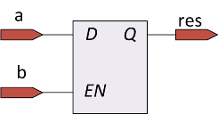
Non-blocking assignments
All assignments that we used in the procedural block examples in Verilog are called “blocking” assignments. They work in a familiar way to the programmer.
In addition to blocking assignments, Verilog has another type of assignment used in procedural blocks — non-blocking assignment, denoted by the <= operator. Non-blocking assignment is not performed immediately, in the place where it is declared, but is postponed until exiting the procedural block. Consider an example:
reg a,b;
always @( posedge clk)
begin
a <= b;
b <= a;
end
In this example, on each clock cycle, the signals a and b will exchange values. The synthesized scheme will look as follows:
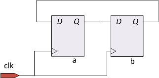
Non-blocking assignments are usually used when describing the logic of register operation. Blocking assignments are more often used to describe combinational schemes.
Conclusion
This concludes the small introduction to Verilog. I hope someone it was useful.
For those who want to get acquainted with Verilog and the design of digital circuits a little deeper, I can recommend these two books for beginners:
Source: https://habr.com/ru/post/137643/
All Articles