An inside look: Flash and RAM

Foreword
The New Year is a pleasant, bright holiday, on which we all sum up the year of the past, look to the future with hope and give presents. In this regard, I would like to thank all the residents of Habra for the support, assistance and interest shown in my articles ( 1 , 2 , 3 , 4 ). If you once did not support the first one, there were no subsequent ones (already 5 articles)! Thank! And, of course, I want to make a gift in the form of a popular science-educational article about how to use fun, interesting and useful (both personal and public) analytical equipment that is rather harsh at first glance. Today, on New Year's Eve, the festive operating table is: A-Data USB flash drive and Samsung's SO-DIMM SDRAM module.
Theoretical part
I will try to be as brief as possible, so that we all have time to prepare the Russian salad with a margin for the festive table, so some of the material will be in the form of references: if you want, you read it at your leisure ...
')
What memory happens?
At the moment there are many options for storing information, some of them require constant electricity (RAM), some are permanently “sewn” into the control chips of the equipment surrounding us (ROM), and some combine the qualities of those and others (hybrid). The latter, in particular, belongs to flash. It seems to be a non-volatile memory, but the laws of physics are difficult to cancel, and periodically you have to rewrite information on flash drives.
Here you can learn more about the below diagram and a comparison of the characteristics of various types of "solid-state memory." Or here - it is a pity that I was still a child in 2003, they did not allow me to participate in such a project ...

Modern types of "solid-state memory". A source
The only thing that, perhaps, can unite all these types of memory is a more or less identical principle of operation. There is some two-dimensional or three-dimensional matrix, which is filled with 0 and 1 approximately in this way and from which we can subsequently either read these values or replace them, i.e. All this is a direct analogue of the predecessor - the memory on ferrite rings .
What is flash memory and how does it happen (NOR and NAND)?
Let's start with flash memory. Once upon a time a rather detailed article was published on the well-known ixbt about what constitutes Flash, and what 2 basic varieties of this type of memory are. In particular, there is NOR (logical non-or) and NAND (logical non-and) Flash memory (everything is also described in great detail here), which differ somewhat in their organization (for example, NOR is two-dimensional, NAND can be three-dimensional) , but have one common element - a floating gate transistor.
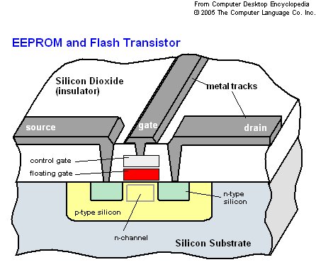
Schematic representation of a floating gate transistor. A source
So how does this engineering marvel work? Together with some physical formulas it is described here . In short, between the control gate and the channel through which the current flows from the source to the drain, we place the floating gate surrounded by a thin layer of dielectric. As a result, when current flows through such a "modified" field-effect transistor, a part of high-energy electrons tunnel through a dielectric and find themselves inside a floating gate. It is clear that while the electrons were tunneling, wandering inside this gate, they lost some of the energy and almost could not return back.
NB: “practically” is the key word, because without rewriting, without updating the cells at least once every few years, Flash is “reset” just like RAM, after turning off the computer.
In the same place, on ixbt, there is one more article which is devoted to the possibility of recording several bits of information on a single transistor with a floating gate, which significantly increases the recording density.
In the case of the flash drive we are considering, the memory will naturally be NAND and, most likely, a multi-level cell (MLC).
If it is interesting to continue to get acquainted with the technology of Flash-memory, then here is a look from 2004 on this issue. And here ( 1 , 2 , 3 ) some laboratory solutions for the memory of a new generation. I don’t think that these ideas and technologies have been implemented in practice, but maybe someone knows better than me ?!
What is DRAM?
If someone has forgotten what DRAM is, then you are welcome here .
Again we have a two-dimensional array, which needs to be filled with 0 and 1. Since the accumulation of charge on the floating gate takes quite a long time, in the case of RAM, a different solution is used. The memory cell consists of a capacitor and a conventional field-effect transistor. At the same time, the capacitor itself has, on the one hand, a primitive physical device, but, on the other hand, is non-trivially implemented in hardware:
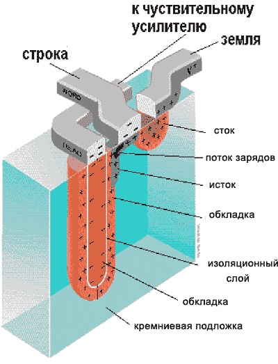
RAM cell device. A source
Again, ixbt has a good article on DRAM and SDRAM memory. Of course, it is not so fresh, but the fundamental points are described very well.
The only question that torments me is: can a DRAM have, like a flash, a multi-level cell? It seems yes , but still ...
Part practical
Flash
Those who use flash drives for quite some time have probably already seen a “bare” drive, without a case. But I still briefly mention the main parts of the USB-flash drive:
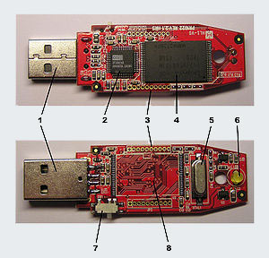
The main elements of the USB-Flash drive: 1. USB-connector, 2. controller, 3. PCB-multilayer PCB, 4. NAND memory module, 5. quartz oscillator reference frequency, 6. LED-indicator (now, however, on many there is no flash drive), 7. write protection switch (similarly, many flash drives are missing), 8. space for an additional memory chip. A source
Let's go from simple to complex. Quartz generator (more about the principle of operation here ). To my deep regret, the quartz plate itself disappeared during polishing, so we only have to admire the body.
Crystal oscillator case
Accidentally, in between times, I found what the reinforcing fiber inside the PCB looks like and the balls, of which the textolite is in its mass. By the way, while the fibers are still laid with a twist, it can be clearly seen in the upper image:

Reinforcing fiber inside the PCB (the red arrows indicate the fibers, perpendicular to the section), from which the bulk of the PCB consists
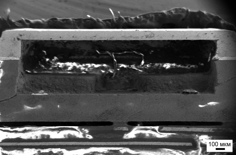
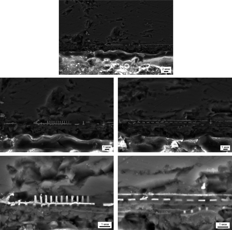
And here is the first important part of the flash drive - the controller:

Controller. The top image is obtained by combining several SEM micrographs.
I admit honestly, I didn’t quite understand the idea of the engineers, who in the pot pouring some more additional conductors. Maybe from the point of view of the technological process it is easier and cheaper to do this.
After processing this picture, I shouted: “Yayayayayaz!” And ran around the room. So, your attention is represented by the 500 nm process technology in all its glory with perfectly drawn boundaries of the drain, the source, the control gate and even the contacts are preserved in relative integrity:

“Ide!” Microelectronics - 500 nm controller technical process with beautifully traced separate drains (Drain), sources (Source) and control gates (Gate)
Now we proceed to the dessert - memory chips. Let's start with the contacts that feed this memory in the truest sense of the word. In addition to the main (in the picture of the “thickest” contact), there are also many smaller ones. By the way, "thick" <2 diameters of a human hair, so everything in the world is relative:

SEM images of the contacts feeding the memory chip
If we talk about the memory itself, then here we are also waiting for success. It was possible to shoot individual blocks, the boundaries of which are highlighted with arrows. Looking at the image with the maximum magnification, try to stretch the view, this contrast is really difficult to see, but it is in the image (for clarity, I marked a separate cell with lines):
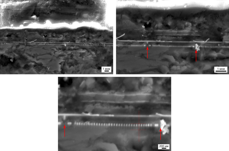
Memory cells 1. Block boundaries are marked with arrows. Lines denote individual cells.
I myself first thought it was an image artifact, but after processing all the photos of the house, I realized that these were either control valves extended along the vertical axis in the SLC-cell, or they were several cells collected in the MLC. Although I mentioned MLC above, this is still a question. For reference, the “thickness” of the cell (i.e. the distance between two bright points in the lower image) is about 60 nm.
In order not to be cunning - these are similar photos from the other half of the flash drive. Completely similar picture:

Memory cells 2. Block boundaries are marked with arrows. Lines denote individual cells.
Of course, the chip itself is not just a collection of such memory cells, inside it there are some other structures, the identity of which I could not determine:
Other structures inside NAND memory chips
DRAM
Of course, I didn’t cut the entire SO-DIMM from Samsung, only with the help of a construction hair dryer I “unplugged” one of the memory modules. It is worth noting that one of the tips suggested after the first publication came in handy - cut at an angle. Therefore, for a detailed immersion in what you see, this fact must be taken into account, especially since cutting at 45 degrees made it possible to get “tomographic” slices of a capacitor.
However, according to tradition, we start with contacts. It was nice to see what BGA looks like and what the soldering itself is:

"Chip" BGA-soldering
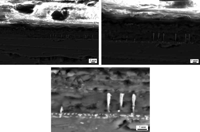
And here it is time to shout for the second time: “Ide!”, Since we managed to see separate solid-state capacitors - concentric circles on the image, marked with arrows. It is they who store our data while the computer is running as a charge on its plates. Judging by the photographs, the size of such a capacitor is about 300 nm in width and about 100 nm in thickness.
Due to the fact that the chip is cut at an angle, some capacitors are neatly cut in the middle, while others cut only the “sides”:

DRAM memory in all its glory
If someone doubts that these structures are capacitors, then you can look at a more “professional” photo (though without a large-scale tag).
The only moment that confused me was that the capacitors were arranged in 2 rows (bottom left photo), i.e. it turns out that there are 2 bits of information per cell. As mentioned above, information on multi-bit recording is available, but how much this technology is applicable and used in modern industry remains for me questionable.
Of course, besides the memory cells themselves inside the module there are also some auxiliary structures, the purpose of which I can only guess:
Other structures inside the DRAM chip
Afterword
In addition to those links that are scattered in the text, in my opinion, this review is quite interesting (albeit from 1997), the site itself (and the photo gallery, and chip-art, and patents, and many, many things) and this office , which actually engaged in reverse engineering.
Unfortunately, a large number of videos on the production of Flash and RAM could not be found, so you have to be content with only assembling USB flash drives:
PS: Once again, Happy New Year, the black water dragon !!!
Strangely it turns out: I wanted to write an article about Flash one of the first, but fate decided otherwise. Having crossed your fingers, let's hope that the following, at least 2, articles (about biological objects and displays) will be released in early 2012. In the meantime, the seed - carbon tape:

Carbon tape, on which the samples were fixed. I think that the usual tape looks the same way.
First , the full list of published articles on Habré:
Opening the Nvidia 8600M GT chip , a more detailed article is given here: Modern chips - a view from the inside
An inside look: CD and HDD
An inside look: LED bulbs
An inside look: the LED industry in Russia
An inside look: Flash and RAM
An inside view: the world around us
An inside look: LCD and E-Ink displays
An inside look: matrix digital cameras
An inside look: Plastic Logic
An inside look: RFID and other tags
An inside look: graduate school at EPFL. Part 1
An inside look: graduate school at EPFL. Part 2
An inside view: the world around us - 2
An inside view: the world around us - 3
An inside look: the world around us - 4
An inside look: 13 LED lamps and a bottle of rum. Part 1
An inside look: 13 LED lamps and a bottle of rum. Part 2
An inside look: 13 LED lamps and a bottle of rum. Part 3
An inside look: IKEA LED strikes back
An inside view: are Filament lamps good for you?
and 3DNews:
Microview: a comparison of modern smartphones displays
Secondly , in addition to the blog on HabraHabr , articles and videos can be read and viewed on Nanometer.ru , YouTube , and Dirty .
Thirdly , if you, dear reader, liked the article or you want to stimulate writing new ones, then act according to the following maxim: “pay what you want”
Yandex.Money 41001234893231
WebMoney (R296920395341 or Z333281944680)
Sometimes briefly, and sometimes not so much about the news of science and technology, you can read on my Telegram channel - welcome;)
Source: https://habr.com/ru/post/135515/
All Articles