An inside look: the LED industry in Russia

Hello to all Habra users!
Publication of an article on Habré on parsing LED bulbs from different manufacturers raised a significant wave, both from one of the leading "domestic" manufacturers of LED-lamps, Optogan company, and from ordinary users (almost 200 comments are a joke). There was a lot said, both good and bad. Immediately after the publication of that article, the nanotechnology forum was held under the auspices of RosNano, where it was possible to talk with representatives of Optogan and get some comments. A little later there was an exhibition Interlight, which I could not attend, then an LED conference in Skolkovo (“The Second Scientific Conference of the Energy Efficient Technologies Cluster”). In short, there are many events, and, bearing in mind the previous article, I am in a hurry to share with everyone who will be interested thoughts about the LED industry in Russia.
')
The publication will be conditionally divided into two parts: an interview with Vladislav Bugrov, the executive director of the Optogan company, and some generalization of the material accumulated over the past month and a half.
I know that many habrazhiteli love to delve into the problem until the very end - this is how Optogan began .
Part one. The long-awaited comments of representatives of the company "Optogan"
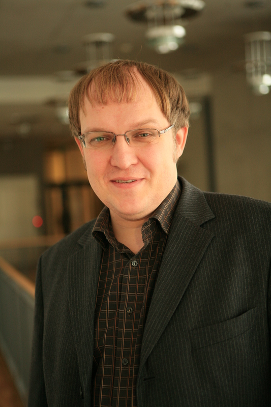
Vladislav Bugrov, Executive Vice President, Optogan *
Why is Optolux E27 using polycarbonate instead of glass? Despite the fact that the glass is about 2.5-3 times heavier than polycarbonate, it takes much more material to make a “bulb” (it is made of thick polycarbonate) than a glass diffuser, and thus the total weight This part of the lamp turns out to be comparable. In addition, due to the large bulb, and the need for a separate site for its “gluing”, the size of the aluminum radiator is increased, which also affects the cost and weight of the lamp.
We made a diffuser for a lamp made of frosted polycarbonate for two reasons: firstly, this material is unbreakable, and secondly, it is cheaper.
And how much cheaper can you give prices for glass and polycarbonate used by Optogan?
We, like any other manufacturer, do not disclose the cost structure of our products, polycarbonate costs us about 20% cheaper than glass. Although, of course, it all depends on the desired characteristics and the shape of the lens. Admittedly, glass has an advantage in something, in particular, it has better transmittance. For example, matte polycarbonate, which gives uniform light scattering, absorbs about 15%, while matte glass with similar characteristics - 9-10%. In principle, in the future we plan to use glass for some lamps, and polycarbonate for some lamps. While it was important to make the light bulb unbreakable, because as it turned out, the first thing that everyone (including you) checked was how it will fight.
The housing of the LED modules manufactured by Optogana OLP-X5050F6 * is similar to the cases of SvetaLED (SVL03P1-FX-XX). Are these cases purchased from third-party manufacturers or is it the development of Optogan?
In addition to the production of Chip-on-Board modules (at the recently concluded Interlight exhibition, Optogan Company presented the second generation of COB ), like the one used in the O27 lamp E27, sells LEDs, for which it buys products from third-party manufacturers, so the visual a coincidence may be. And not only at Optogana and Svetlana, but also in the overwhelming majority of global manufacturers. The difference in this case is in which LED chip is used inside the standard case, as well as in the applied silicones and phosphors (in this case, Mr. Bugrov means “gel” -fill based on silicone and phosphor).
I repeat that in the Optolux light bulb a light source is not a board with discrete LEDs, but a single LED module. In this module, developed by us, there is no plastic case, and such a module is an example of an integral solution that we actively promote in the market.
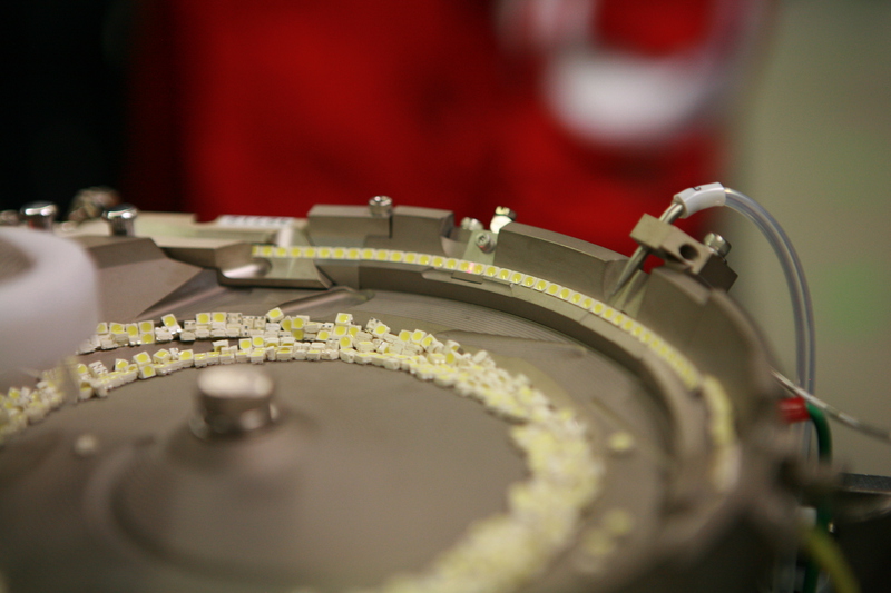
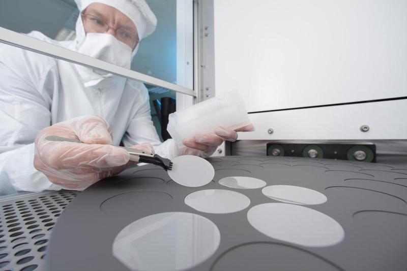
Standard enclosures with LEDs from OptoGan before packing into tape *
How does the company plan to reduce the price of finished products by 2 times?
Very simple: through economy of scale. Although this is not always enough. Now I’m everywhere promoting (at the round table, in many interviews, at Interlight I told) - I have to go to integral solutions. The first step you saw. If you disassemble the bulbs of different manufacturers, then the vast majority of you will see individual LEDs, as well as an individual driver, consisting of individual electronic components. And whatever one may say, but it turns out that a large number of discrete elements are used. And we have taken the first step towards an integral solution - we have developed an integral light module (COB).
The next step is to develop an integrated driver, and then we will try to combine different modules into one solution. This is similar to switching to chips in due time. Once there were computers that occupied entire rooms and even buildings. Then they invented semiconductor chips. Now the cost of microcircuits varies from hundreds of dollars per processor to units of dollars for some simple solutions. In lighting will be about the same. Here is our philosophy.
Perhaps a COB solution with a large LED alone is not justified (for example, the heat sink is deteriorating, which could potentially lead to premature "wear" of the LED module)? Maybe it was worth to follow the path of world market leaders?
Because COB, i.e. integrated solution, just allow to reduce the price in the future. About the deterioration of the heat sink - this is an erroneous statement.
The thermal resistance of the currently most used 0.5 W LED in the 5630 Rjs package (junction-solder point) is approximately 40-60 K / W. When landing this LED even on a metal board with a small thermal resistance (typical values 1-4 K / W), due to the presence of passivation layers separating the contacts with the base, the total resistance Rjb (junction-board) will be the sum of the board's resistance and LED, i.e. approximately equal to the thermal resistance of the LED (at best, 7K / W, in typical applications> 40K / W).
In the SOW module, the chips are planted directly on a metal base, which allows Rjb (junction-board) to be <1K / W on large chips and 2-3K / W on small ones. Accordingly, SOW provides less thermal resistance between the chip recombination zone and the external environment than on the board with LEDs, which obviously provides an improved heat dissipation when compared with the widely used technology.
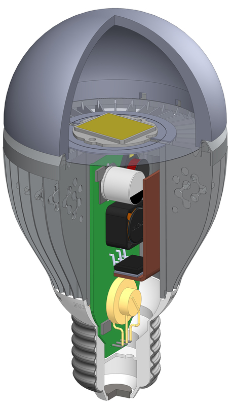
Lamp Optolyuks E27, in which applied COB-solution *
That is, the aluminum substrate copes well with the heat sink?
Yes, besides, it does not have to be made of aluminum or copper. For example, you can use ceramic substrates. In the simplest case, it is ceramics based on aluminum oxide or nitride. Many manufacturers (CREE, OSRAM OS, Nichia, LumiLEDs) recently began to use it in the manufacture of their LEDs. For example .
The difference is in the detailed compositions of ceramics that make up the technological “know-how” of material manufacturers. At the Interlight were presented and our SOW on ceramic substrates. It should be noted that the thermal conductivity indicators for them turned out to be better than for metal substrates.
But isn’t the driver warming up while working, is he so tightly packed?
The driver, of course, heats up during operation, however, the main heat is produced by the light source. Driver efficiency is about 85%, light source efficiency is less than 50%. Strategically, we are moving towards greater integration. It is not just about reducing the size, but about reducing the number of components due to the high degree of integration of the latter. This is our philosophy, the direction of further development.
This means that the philosophy of the Optogan company can be described as follows: every year a new iphone or htc appears, which costs about $ 1,000. A year later, it already costs $ 500, but there is a new model for $ 1,000. Translating to a lamp. Today we released a lamp for 1000 rubles from 1% of pulsations, and a year later we will make a “nano” lamp (the claims are mostly in size) with 0.5% of pulsations for 1000 rubles, and we will sell this one for 500 ... Well, microelectronics it works ... Or do you still want to make chip-on-board + driver-on-board = optolux ?! Tell me, did anyone figure out the transition to "integral" solutions? In my opinion, purely subjective, not always integral solutions give significant advantages and reduce the cost of production ...
The size of the radiator will decrease automatically as soon as the efficiency of the light module increases - the size of the radiator is determined solely by the area required for the dissipation of excess heat. The more efficient the light module, the more energy is converted into light and, accordingly, less into heat, and there is no need to use a large radiator.
In the rest - our strategy is aimed at the general reduction in the cost of replacement lamps and the improvement of their parameters (such as dimurability, color rendition and light emission angle). We do not plan to produce light bulbs that will be more expensive than existing ones, which is why we are looking for ways to reduce the cost of the product while improving its characteristics.
If we talk about integrated solutions in microelectronics, they did not always lead to cheaper production, but always led to cheaper final products, which is our goal.
One can understand the economic component of the integral solution using a simple example comparing the light source on LEDs and Chip-on-Board (PSB): if we leave aside the issues of economy of scale and the existence of existing production lines, we see the following at the level of LED modules.
At the level of elementary components, the board with LEDs is:
1. the board itself,
2. LED chips which
3. packed in plastic cases
4. Each chip is contacted to the case contacts.
5. housing planted on the board.
In the SOC module there are no plastic cases, the chips are mounted directly on the board, thus, points 3 and 5 disappear. For the sake of justice, it should be noted that the PSU uses more silicone with phosphorus mixed in it than in the board with soldered LEDs, but in the end the cost OWL is still lower than the board with LEDs (depending on the design, the difference can be up to 50%).
The peculiarity of the current moment lies in the fact that in the world there are too many lines for the production of LEDs and too little for the production of modules PSB. Given the crisis of overproduction of LEDs designed to illuminate TFT monitors and TVs, manufacturers of these LEDs staged a real dumping war, selling LEDs at cost level. This situation is temporary and will change after the ruin of a large number of small manufacturers of similar LEDs and market consolidation, which will occur within the next year.
During the same time, manufacturers will increase their production capacity for PSI modules (this trend is clearly observed, just look at the total number of companies offering PSB modules a year ago and now) and everything will fall into place, that is, PSB modules will become cheaper than modules on assembled LEDs.
Will hope. Do you plan to conduct R & D in the field of minimizing the driver and reducing the size of the lamp? Why is your driver the biggest?
Together with our partners, we are already carrying out R & D in the field of integral solutions for the driver, which will lead to a decrease in its size, and with an increase in the efficiency of the light-emitting module and a reduction in the size of the whole lamp. At the moment, our driver is not only the biggest, but also the best, we provide a level of pulsation that no other manufacturer can do.
This is good, but are there any studies that confirm that the pulsations of 1% and 3% differ significantly among themselves in their effects on the body?
Between 1% and 3% the difference is insignificant, however, between 1% and 10% is already significant. Studies on the effects on the body is enough. For example, one of the reports .
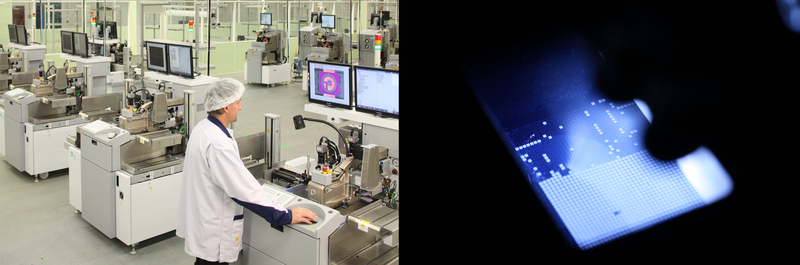
Installation for installation of individual LEDs in the modules. Judging by the photo - large crystals measuring about 1 mm by 1 mm *
Is the phosphor used in the Optogan lamps manufactured in Russia?
We have worked with many manufacturers of phosphors and now we are focused on products made in Germany and the USA. There are also interesting firms in Russia, but so far we have not used their products in our production. First, oddly enough, but it turned out that domestic phosphors are more expensive than imported ones ...
Did you analyze why such a strange tendency appeared?
“Why” domestic phosphors are more expensive; this is probably a question for manufacturers of phosphors. If we compare the parameters, then, from an objective point of view, they should be cheaper. Apparently, the turnover is not large enough to offer goods at a lower price.
Although the price difference is not decisive. The most important thing: domestic phosphors can not fully meet our needs. Domestic companies have some successful luminophores, but for the production of a large set of different luminaires with different luminous characteristics, a rather wide range of luminophores is needed. Unfortunately, we don’t find such a wide range of products at any domestic supplier. Although, I see a very noticeable development in the production of domestic phosphors and, if in the near future the situation changes for the better, we will actively use them in our production.
Is it not easier to buy the phosphor in China, because it is a rather expensive element of the structure?
The quality is worse. This component is expensive, but now all prices are such that it does not determine the price of our products. And the quality of Chinese products is still noticeably worse. In general, while American and German are the best that we have found for ourselves. It was more important for us to provide exactly the quality of the products. But we periodically test various phosphors and it is clear that Chinese manufacturers are quickly catching up to the leaders.
However, it is worth noting that the production of phosphors is the industry that is likely to be created in the near future in Russia, because it does not require large investments in equipment. We need the knowledge, the necessary skills, the chemistry of the processes - this is all we have, so the forecast for the development of such domestic production is positive.
As far as I know, problems with phosphors in rare earth elements (REE), which are used to produce them. And in Russia there are few deposits where REEs would be mined, they are mainly concentrated in the territory of China.
This is not quite true: in the CIS countries (mainly Russia and Kazakhstan) there are 19% of the world reserves of REE, in China - 38% (for details here )
By the way, the problem with the “availability” of REE is not always the main one.
What else ?!
For example, the purity of the materials used and the size of the granulate are important.
If possible, tell us in more detail about phosphors, quantum dots, rare earths and silicates ...
Let's go back to the phosphors.
As you know, to convert the blue light emitted by LED chips into white, various phosphors (phosphors) are used, which are divided into various classes.
So widely used in our production of YAG-phosphors ( Yttrium aluminum garnet - yttrium-aluminum garnet Y 3 Al 5 O 12 ) and silicates contain rare earth elements. YAG contains yttrium, which belongs to rare-earth elements, and is doped with Ce ions. In addition, some manufacturers include other rare-earth elements along with or instead of yttrium in the composition of YAGs and their analogues.
The composition of silicates with REE includes only Europium. Compared to YAG-phosphors, the REE content in silicates is lower, since there they are not included in the matrix, but are only a dopant (with a concentration of <2%).
Rare earth metals and their compounds are low hazard and non-toxic substances. All the phosphors we use have safety certificates (MSDS) confirming their safety for the human body.
But the phosphors on quantum dots of rare earth materials do not contain. These are usually compounds of sulfur, zinc, cadmium, selenium (for example, CdSe, CdS, ZnCdSe, and others). We do not use similar phosphors in our products yet, however we are actively developing in this direction.
How many installations of MOCVD the company has already installed, and how many plans to put into circulation in the coming year in the territory of the Russian Federation?
It is no secret that we have only five installations, and all of them are in Germany. In Russia, we are not launching production yet, because there are problems in the country with the supply of pure materials necessary for the epitaxial growth of semiconductor structures, at a reasonable price. In particular, pure ammonia is 10 times more expensive than in Germany. And the price pressure is huge due to the strong competition from Chinese and Taiwanese manufacturers.
While in Russia we produce LEDs, electronics and lamps, but we also gradually localize the production of LED chips. We plan that it will be launched in Russia next year. While it is economically more profitable.
And the substrate initially somewhere to buy?
Yes, we buy sapphire substrates. Next we buy gases and organometallic compounds containing gallium, aluminum and indium. And, accordingly, we ourselves grow semiconductor structures on substrates in MOCVD reactors.
Here they are the same sapphire substrate ... *
Do you deliver to Russia and cut already here?
So far, and cut in Germany. From next year we will be cut in Russia.
Is the company ready to demonstrate the plant in the Russian Federation with a full production cycle (from the processing of sapphire plates to the packaging of LED modules)? Will you invite us to the factory?
Of course, we will invite, believe me, there are many interesting things.
If we talk about the full cycle, then we will be able to show the processing of plates in St. Petersburg next year. Epitaxial growth is a separate issue in which we are still looking for a compromise.
Holy of holies of the domestic LED industry *
Part two. A fly in the ointment: everyone drags a blanket over himself
In order not to constantly refer to the decisions of the two conferences of the 7th and 8th "Gallium, Indium and Aluminum Nitrides: Structures and Instruments" in the course of the narrative , I would like to immediately refer to them. Conference proceedings .
At least two disappointing conclusions can be drawn from the interview with Vladislav Bugrov :
1. The absence of MOCVD installations in Russia is due primarily to the inability to purchase at reasonable prices clean gases and reagents required for precipitation.
2. Despite the reserves of REE elements necessary for the synthesis of high-quality phosphors in Russia and Kazakhstan, we are not able to ensure their “transformation” into cheap and affordable materials for subsequent industrial use in the LED industry.
As for the first conclusion, then you can only shrug. An entire network of intermediaries is often built up between the producer and the consumer, each of whom wants to get their own from 5 to 30 percent of the profits. Although our country is often called the “raw materials appendage” of the world economy, in fact it turns out that we are even worse. At the moment, we (the state or private investors - this is not so important) could not create an infrastructure in our country that allows producing the same pure gases. But the energy efficiency program was adopted by the party (cross out) and the government at the end of 2009. Suppose for 2 years we were able to build only an enterprise, which, in fact, is engaged in a “screwdriver” assembly, but, nevertheless, let's say together the Optogan and Svetlana companies thank you so much! - this is a really great achievement.
, , - . ( - , – , - - - ). , , -94, .. , .
, 8- : « In general, the problems of the industry, identified one and a half years ago at the previous Conference, have not changed or even worsened. First of all, this refers to the country's institutions for the development of science, the 94th Federal Law, the strategic instability in the Russian market of high-tech materials, personnel shortage, aggravated by demographic problems, extremely low decision-making speed . ”
, , , . , , . , , – – . 7- (. .5) .
, – « » , . , , , , , «» . , , «» : ( MOCVD) - , - – .
, , . , , – «», . , , , , - - .
, , , («» , , , ..), «» , . Those.to manufacture products created outside our homeland, but under the domestic brand and proudly writing “Made in Russia”. If we want with a clear conscience to write this truly historical inscription, then the entire technological chain MUST be carried out within our Motherland.
However, in order to understand what the consequences in the field of the LED industry "tactical" approach can lead, it is enough to recall the end of the 80s and Elbrus processors (as one of the vivid examples). Literally in one decade, our country moved from the “non-contributory” in the development and production of computer equipment to the category of “highly dependent on imports” of this very technology.
Once again, the company "Optogan" and "Svetlana" - great lads , , ! , - «» , , hi-tech ( , MOCVD), …
, , ( , – , , ?!), , …
Afterword
1. - , «» ( ).
2. (, ).
3. , , ?! , , , - , , , , .. (2D), ( , ), . , , , , …
4. Just the other day in the December issue of GQ magazine, an article in the “Made in Russia” section appeared with a rather detailed interview with the president and CEO of Optogan, Maxim Odnoblyudov.
5. Despite all the pressure from the press service of Optogana (almost an hour of telephone conversations), which was extremely huge, I did not at my own risk change anything in the final version of the publication. Forgive me, optoganovtsy, I can only write the truth: what I consider important, interesting, as well as what I see with my own eyes!
PS : , . , , , , , , , «»
PPS : , , , , , flash- DRAM-. (, ). , , 2 – , , , ! , , c Crysis 2.
* - «».
** portalnano.ru .
First , the full list of published articles on Habré:
Opening the Nvidia 8600M GT chip , a more detailed article is given here: Modern chips - a view from the inside
An inside look: CD and HDD
An inside look: LED bulbs
An inside look: the LED industry in Russia
An inside look: Flash and RAM
An inside view: the world around us
An inside look: LCD and E-Ink displays
An inside look: matrix digital cameras
An inside look: Plastic Logic
An inside look: RFID and other tags
An inside look: graduate school at EPFL. Part 1
An inside look: graduate school at EPFL. Part 2
An inside view: the world around us - 2
An inside view: the world around us - 3
An inside look: the world around us - 4
An inside look: 13 LED lamps and a bottle of rum. Part 1
An inside look: 13 LED lamps and a bottle of rum. Part 2
An inside look: 13 LED lamps and a bottle of rum. Part 3
An inside look: IKEA LED strikes back
An inside view: are Filament lamps good for you?
and 3DNews:
Microview: a comparison of modern smartphones displays
Secondly , in addition to the blog on HabraHabr , articles and videos can be read and viewed on Nanometer.ru , YouTube , and Dirty .
Thirdly , if you, dear reader, liked the article or you want to stimulate writing new ones, then act according to the following maxim: “pay what you want”
Yandex.Money 41001234893231
WebMoney (R296920395341 or Z333281944680)
Sometimes briefly, and sometimes not so much about the news of science and technology, you can read on my Telegram channel - welcome;)
Source: https://habr.com/ru/post/135155/
All Articles