PCB manufacturing process at home
Introduction
Who didn't have to make a PCB? This is not a very complicated matter, but the result gives the project completion. In this post I would like to talk about the process of creating a printed circuit board at home. I will describe the photoresistive method of creating the board. It is quite simple to use and allows you to print very complex boards. Moreover, I managed the inkjet printer.
The post contains photos, videos and schemes.
The idea of a photoresistive method is very simple. Copper on the PCB on top is covered with a special substance. If light gets on this substance, then it is dissolved in the developer. If the light does not hit, then the substance remains in the developer dye. The manufacturing process of the board consists of four parts:
1. Create a transparent mask on which it is marked what to connect to.
1. Light on the board with the substance through this mask
2. We throw the board into the developer: only the places marked on the mask are painted on the board
3. We throw the board into the etchant: it will eat all the copper, except the painted one.
Creating a schema
The first step in creating a printed circuit board is quite obvious: you need to create a diagram of what will be on the board. A pretty standard program for this is Eagle CAD . Despite the fact that the program is quite difficult to master (it seems to me that it is absolutely disgusting to use), many people use Eagle CAD. There are so many users that manufacturers and parts suppliers sometimes create component libraries.
')
As part of this post, we will make a fairly simple device: a board distributing contacts for ATTiny. So that you can plug in the chip, power and programmer.
First, we draw a simple scheme, and then, by clicking “Switch to board”, we place the components on the board layout.


Scheme and wiring board can be seen here .
Print layout
Prepare a layout for printing. You need to make sure that only layers with Bottom, Pads, Vias, Dimension are included. In the print menu, you must enable Mirror and Black. Thus, the layout will be reflected and printed only in black. I don’t know if there is a more convenient way, but I printed the layout in PDF, converted PDF to TIFF with a fairly decent resolution, and then in a text editor I duplicated the image to fill in the sheet:

I note that I printed two schemes, one for today, and the other for later.
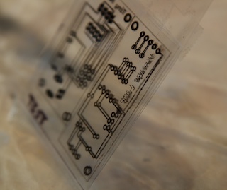
The document is ready. We print on a transparent film. I used a film from MG Chemicals . Although it was designed for laser printers, I used my Lexmark inkjet. Minus: it is easy to smear ink.
Board preparation
It is obvious that for the photoresistive process a charge is required that is coated with a special substance. You can buy this substance and cover the board yourself, but I decided to buy the finished one . Cut a piece of the board according to the size of the circuit. I used a Dremel machine for cutting:

Exposure
Everything is ready for exhibiting the board. Experience shows that an inkjet printer may not give the desired density (that is, black in appearance will actually be riddled with small holes). To deal with this is not difficult: you can combine two or three layers of printout. Like this:

We remove the protective layer from the board (white thin film) and put it on the base (the electronics book gives us a good luck score of +3). We will cover the board with a film with a printout and press this case with glass:

The design should stand under a strong lamp for 10 minutes:

Developing
While the board is on display, we will dilute the developer. The developer box contains the proportion and recommended temperature. I took a developer from MG Chemicals . He gets divorced in any plastic pot in the ratio of 1 to 10:

The developer is ready, ten minutes have passed. We take the fee and throw it into the developer:
It turns out something like this:

Etching
We rinse the board in the water and throw it into the etchant. I used ferric chloride from MG Chemicals . The recommended temperature is 50 ° C, but I poisoned at room temperature 25 ° C. It took 20 minutes:
It turns out something like this:

Sweep
The remaining dye is easily removed with spirited rags:
As a result, there is a clean fee:

Holes
Holes to make holes easy. I used the same Dremel machine :
It turns out almost ready fee:

Components
We cling to the board the necessary components and solder them to the copper base:

Result
The fee turned out right, even though friends show:

However, not all friends will explain what it is ...
Security
The process of making boards using this method involves working with all kinds of chemical rubbish.
First of all, do not pour chemical rubbish into a sink or toilet. There are a lot of tips on the Internet about what to do with this rubbish.
Secondly, this chemical rubbish spoils clothes, leaves stains on hands and does something absolutely terrible with eyes. Please use security features! For example, I used rubber gloves, glasses and an apron from a shower curtain:

I will be happy to answer questions, hear suggestions how this process can be improved, and, of course, to supplement the post with any missing information.
Source: https://habr.com/ru/post/134834/
All Articles