Programmer for FPGA
I want to talk about how the project http://marsohod.org is developing.
The goal of the project is to popularize the design for the FPGA.
The FPGA theme is gradually gaining popularity - and quite deservedly. After all, now we actually got a simple opportunity to create our own digital microcircuit. You do not need a nano-fab and a million dollars - everything can be done simply by having a computer and an FPGA chip on the developer's board. Do you know that 90% of the chip manufacturers in the world do not have their own factories? They design and test in FPGA, and the production is ordered to third-party manufacturers.
Once, programming microcontrollers was considered almost a miracle. Now you can buy an Arduino headscarf and teach a high school student to “blink a LED”.
')
I want to show that FPGA is an affordable technology.

The “Mars Rover” board is the easiest and cheapest developer of a whale on an FPGA chip from Altera company EPM240T100C5. The project - open resource - the scheme of the board is on our website. In addition, more than 50 projects published on the basis of our board have been published.
Then I will talk about the programmer for the FPGA. It is believed that learning to design FPGAs is much more expensive than learning microcontrollers. This opinion is partly due to the fact that the programmers of FPGA vendors are quite expensive.
Now there is an alternative. You can make a simple USB programmer yourself!
We have developed a very simple programmer on the FTDI FT2232HL microcircuit. Here is this:
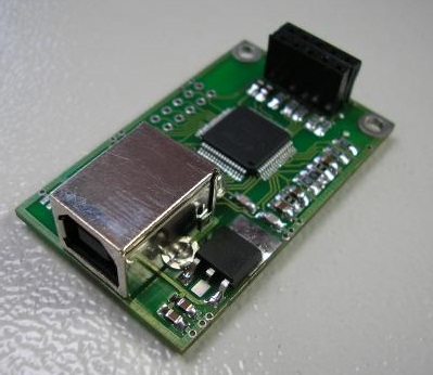
This is a USB JTAG programmer. His scheme is also on the site , so if you want, you can make it yourself:

The software we wrote to it is the SVF Player. Briefly tell how it works.
The design environment for the FPGA Altera Quartus II allows you to create files for programmers in different formats during the compilation of your project: POF, SOF, JAM, SVF. The Xilinx ISE design environment also allows you to create SVF files.
Files in SVF format is a simple text file with the description of commands that need to be transferred to the FPGA chip via the JTAG interface for programming. An SVF (Serial Vector Format) file might look like this:
In the chip behind the JTAG interface, there is a so-called TAP controller that controls the process of testing and programming FPGA chips. The TAP controller has two registers: the IR command register and the DR data register.
The main commands in the SVF file are data transfer to the instruction register (SIR command) and transfer to the data register (SDR command).
For example, the command SIR 10 TDI (203); says that you need to transfer a ten-bit number 0x203 to the IR register. Another example: SDR 16 TDI (FFFF) TDO command (2AA2); says that you need to transfer to the DR register a sixteen-bit number 0xFFFF, but in response, the chip must send the number 0x2aa2. Another important command is RUNTEST. It allows you to withstand pauses of a given duration when programming. Usually pauses are kept in the TAP controller states IDLE, IRPAUSE or DRPAUSE.
Correctly executing commands from the SVF file, you can “sew” the FPGA chip. This is what our program SVF player MBFTDI does.
The JTAG chip programming and testing interface has only four main signals for data transmission: TCK is a clock signal, TMS is a transmission control signal, TDI signal is data transferred to the chip, and TDO is data read from the chip. To transfer data to the TAP registers of the IR and DR controller, you need to understand how to manage the state of this controller. Let's try to figure it out.
In fact, everything is quite simple. The states of the TAP controller are described by such a state machine:

The TAP controller changes its state during a TCK signal pulse and depending on the value of the TMS signal.
For example, it can be seen that in order to reset the TAP controller to the RESET state from any other state, it is enough to hold the TMS in the unit for at least 6 TCK pulses. If you need to go from the RESET state to IDLE, you need to translate the TMS to zero and send at least one TCK pulse. From IDLE to the data transfer state to the SHIFT_IR instruction register is just 4 TCK pulses when the TMS changes to 1-1-0-0.
In our MBFTDI programmer, we use an FTDI FT2232HL chip in which we have already implemented the management of all these JTAG lines. Our MBFTDI SVF player program reads the SVF file, interprets it and sends commands to the FTDI chip controlling the JTAG lines. Description JTAG commands FTDI chip is here .
We have already tested our programmer with Altera MAX II, Cyclone II, Cyclone III series chips and some Xilinx chips.
Of course, the programmer works on both Windows and Linux.
Of course, the source code is available on our website in the download section or on GITHUB .
I hope our project http://marsohod.org will help you quickly master the design for FPGAs.
The goal of the project is to popularize the design for the FPGA.
The FPGA theme is gradually gaining popularity - and quite deservedly. After all, now we actually got a simple opportunity to create our own digital microcircuit. You do not need a nano-fab and a million dollars - everything can be done simply by having a computer and an FPGA chip on the developer's board. Do you know that 90% of the chip manufacturers in the world do not have their own factories? They design and test in FPGA, and the production is ordered to third-party manufacturers.
Once, programming microcontrollers was considered almost a miracle. Now you can buy an Arduino headscarf and teach a high school student to “blink a LED”.
')
I want to show that FPGA is an affordable technology.
The “Mars Rover” board is the easiest and cheapest developer of a whale on an FPGA chip from Altera company EPM240T100C5. The project - open resource - the scheme of the board is on our website. In addition, more than 50 projects published on the basis of our board have been published.
Then I will talk about the programmer for the FPGA. It is believed that learning to design FPGAs is much more expensive than learning microcontrollers. This opinion is partly due to the fact that the programmers of FPGA vendors are quite expensive.
Now there is an alternative. You can make a simple USB programmer yourself!
We have developed a very simple programmer on the FTDI FT2232HL microcircuit. Here is this:
This is a USB JTAG programmer. His scheme is also on the site , so if you want, you can make it yourself:
The software we wrote to it is the SVF Player. Briefly tell how it works.
The design environment for the FPGA Altera Quartus II allows you to create files for programmers in different formats during the compilation of your project: POF, SOF, JAM, SVF. The Xilinx ISE design environment also allows you to create SVF files.
Files in SVF format is a simple text file with the description of commands that need to be transferred to the FPGA chip via the JTAG interface for programming. An SVF (Serial Vector Format) file might look like this:
!
FREQUENCY 10000000.00 HZ;
!
TRST ABSENT;
ENDDR IDLE;
ENDIR IRPAUSE;
STATE IDLE;
SIR 10 TDI (2CC);
RUNTEST IDLE 10003 TCK ENDSTATE IDLE;
!
!CHECKING SILICON ID
!
SIR 10 TDI (203);
RUNTEST 53 TCK;
SDR 13 TDI (0089);
SIR 10 TDI (205);
RUNTEST 53 TCK;
SDR 16 TDI (FFFF) TDO (8232) MASK (FFFF);
SDR 16 TDI (FFFF) TDO (2AA2);
SDR 16 TDI (FFFF) TDO (4A82);
SDR 16 TDI (FFFF) TDO (0C2C);
SDR 16 TDI (FFFF) TDO (0000);
!
!BULK ERASE
!
SIR 10 TDI (203);
RUNTEST 53 TCK;
SDR 13 TDI (0011);
SIR 10 TDI (2F2);
In the chip behind the JTAG interface, there is a so-called TAP controller that controls the process of testing and programming FPGA chips. The TAP controller has two registers: the IR command register and the DR data register.
The main commands in the SVF file are data transfer to the instruction register (SIR command) and transfer to the data register (SDR command).
For example, the command SIR 10 TDI (203); says that you need to transfer a ten-bit number 0x203 to the IR register. Another example: SDR 16 TDI (FFFF) TDO command (2AA2); says that you need to transfer to the DR register a sixteen-bit number 0xFFFF, but in response, the chip must send the number 0x2aa2. Another important command is RUNTEST. It allows you to withstand pauses of a given duration when programming. Usually pauses are kept in the TAP controller states IDLE, IRPAUSE or DRPAUSE.
Correctly executing commands from the SVF file, you can “sew” the FPGA chip. This is what our program SVF player MBFTDI does.
The JTAG chip programming and testing interface has only four main signals for data transmission: TCK is a clock signal, TMS is a transmission control signal, TDI signal is data transferred to the chip, and TDO is data read from the chip. To transfer data to the TAP registers of the IR and DR controller, you need to understand how to manage the state of this controller. Let's try to figure it out.
In fact, everything is quite simple. The states of the TAP controller are described by such a state machine:
The TAP controller changes its state during a TCK signal pulse and depending on the value of the TMS signal.
For example, it can be seen that in order to reset the TAP controller to the RESET state from any other state, it is enough to hold the TMS in the unit for at least 6 TCK pulses. If you need to go from the RESET state to IDLE, you need to translate the TMS to zero and send at least one TCK pulse. From IDLE to the data transfer state to the SHIFT_IR instruction register is just 4 TCK pulses when the TMS changes to 1-1-0-0.
In our MBFTDI programmer, we use an FTDI FT2232HL chip in which we have already implemented the management of all these JTAG lines. Our MBFTDI SVF player program reads the SVF file, interprets it and sends commands to the FTDI chip controlling the JTAG lines. Description JTAG commands FTDI chip is here .
We have already tested our programmer with Altera MAX II, Cyclone II, Cyclone III series chips and some Xilinx chips.
Of course, the programmer works on both Windows and Linux.
Of course, the source code is available on our website in the download section or on GITHUB .
I hope our project http://marsohod.org will help you quickly master the design for FPGAs.
Source: https://habr.com/ru/post/134657/
All Articles