Semiconductor electronics

Semiconductor electronics have significantly changed the world. Many things that for a long time did not leave the pages of the works of science fiction writers became possible. To know how semiconductor devices work and how unique they are, it is necessary to understand the various physical processes that take place inside.
The article discusses the principles of the main semiconductor devices. The description of the functioning set out from the perspective of physics. The article contains an introductory description of the terms necessary for understanding the material to a wide range of readers.
')
Illustration: 34, characters: 51 609.
On Habré recently, a large number of feature articles on various semiconductor devices and their parameters. It is not surprising that this material is especially interesting to beginners in the field of electronics, since the modern abundance of various devices is due to semiconductor electronics. This material should be regarded as some addition to the wonderful articles AveNat , Dooez and IIIa66uMEM6eP , published in this blog. The description given in the article is intended to tell more about the physical side of the issue, although some technical features are also indicated. Among other things, the material overlaps with the already published articles, which is also a plus for students of the material, since information about the same from different lips promotes closer to the truth. Traditionally, the material is designed for a wide range of readers, so the presentation is quite detailed. You can quickly become familiar with the content of the summary paragraphs that are at the end of each section. At the end of the article for those interested are a list of additional sources of knowledge.
Modern electrical devices are very complex devices. The physical details of their functioning are not always easy to understand. In order to clearly understand the principle of operation of a device, it is necessary to know the basic physical phenomena underlying them. Therefore, in order to continue to speak in one language, below is a brief description of such concepts as the electric field, electric current and diffusion.
Step 1. Electric field
From the standpoint of physics, the electric field is some matter that exists “side by side” with charged bodies. It should be noted that such terms as matter, body and charge will not be discussed here, because these are topics of discussion on the verge of physics and philosophy. It should only be understood that this is all connected with the phenomenon of electricity and, accordingly, by a charge is meant an electric charge. For greater clarity, you can look at the figure below.

On the picture there are two objects - balls. Each ball has a special characteristic - the charge. This charge can be either positive or negative. These two balls interact with each other through an electric field that is “around” them. This is the essence of the electric field: it is due to the existence of certain electrical forces between charged bodies. These forces are such that if the balls have charges of the same sign, then they will move away from each other, if different, then vice versa - to approach. The question can be studied in more detail in physical textbooks on the subject of Coulomb's law and the electrostatic field.
For convenience, the electric field is characterized by a special value - intensity. It is needed in order to compare which field is “stronger” and which is “weaker”. What formulas are calculated and in which units is measured in this case is not important. The main thing is that the greater the electric field strength, the “stronger” it acts on a charged body. Also this field characteristic has direction. In this case, it is said that intensity is a vector quantity, since the vector usually has some direction. It is necessary to know the direction in order to determine in which direction the field will “push” the charged body. You can clarify the situation with the help of the figure and one formula.

In the picture one ball placed in an electric field. In this case, it does not matter what charged bodies the field was formed. The field is characterized by tension, which has a certain direction. The ball has a certain charge of a sign. The formula given in the figure suggests that if the charge of the ball is positive, then the field “pushes” it forward (spoken across the field), if negative, then against the field.
The simplest example of a real charged body is an electron. Which, being a purely quantum object and “living” according to “magical” laws, in some approximation can be considered a ball, for which all the arguments above are valid. The electron charge is negative, so it “flies” against the field.
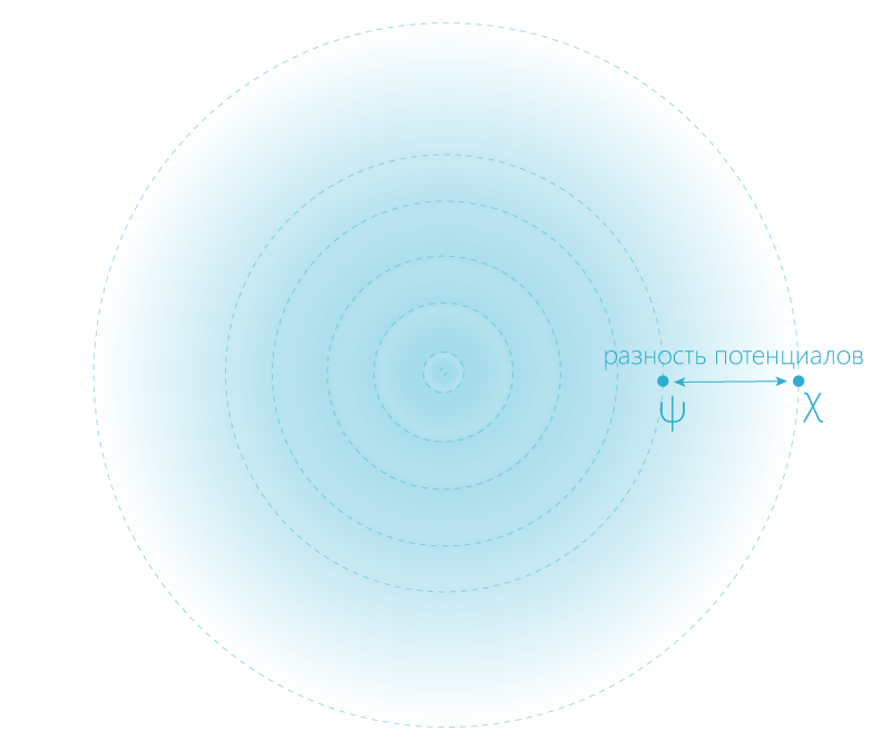
In addition to everything else, besides the strength that describes the power characteristics of the electric field, they introduce another characteristic - the potential. Potential is an energy characteristic. Energy in physics in general is an interesting thing and its understanding also belongs to the category of philosophical and physical discussions. Because of its properties, it is very convenient for mathematical calculations. We will not dwell on this question here.
The potential describes the energy properties of each point where there is a field and in the general case for each point it is different. Of particular interest is the potential difference. There is a connection between the potential difference and the field strength. The essence of this concept can be understood from the figure below. The potential difference is usually referred to as voltage (not to be confused with tension). This is not exactly the voltage that is measured in electrical circuits with a voltmeter, although there is some connection. Again, all the subtleties can be learned from textbooks on physics.
In physics, any movement of charged bodies that has a clear direction is called a current. In this case - an electric shock. It is very important that the movement of charged bodies can occur not only because of the effect of the field on them. Due to the fact that there is a dedicated direction, the current also has some direction. Historically, to move negatively charged particles, the current is considered to be directed in the opposite direction. More on this in the picture.
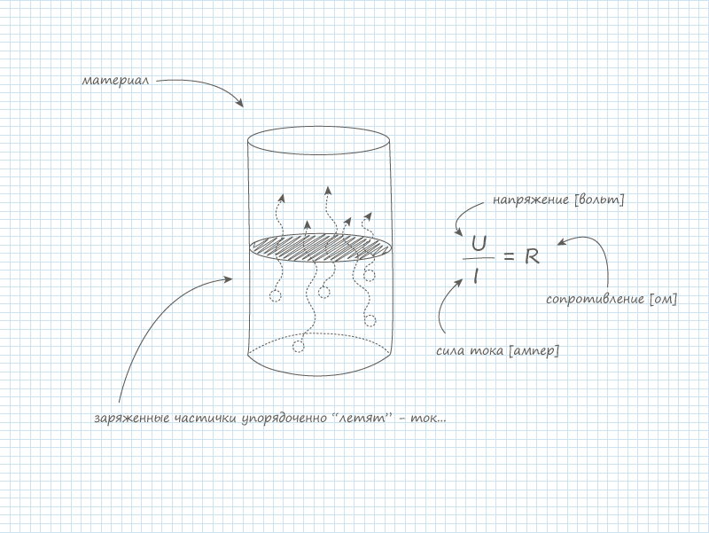
In practice, a quantity is usually used - the current strength, which is simply called a current, and which is measured in amperes . This value describes how many charged bodies “fly through” per unit of time through a certain area (section of material). The relationship between current (amperage) and voltage is determined by Ohm's law (the formula in the picture). These two quantities are related by a coefficient, which is called resistance. This coefficient characterizes the material and various physical phenomena that accompany the current flow in this material. Usually resistance is just a number, although there are more complex cases. This can be read in textbooks. Sometimes, for convenience, they use instead of resistance another quantity - conductivity. The difference between them is clear from the name: the greater the resistance of the material, the worse (less) its conductivity.
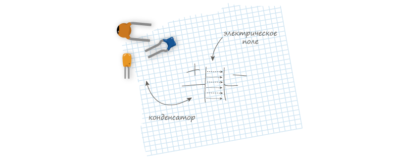
Among electrical phenomena, another very interesting feature is that if there are any accumulations of opposite charges, an electric field (voltage) arises between them, which indicates that such a system stores the energy of the electric field. These systems are numerically characterized by the parameter - electrical capacity. On this principle, the popular electrical devices - capacitors. We will not go into the nuances.
You also need to understand that electrical phenomena are a special case manifestation of electromagnetism, about which you can read more in the literature, which is given at the end of the article.
Summary
At the heart of electronics are various physical phenomena of electrical nature. The most important concepts are the electric field of charged particles and their electric current. The electric field is characterized by tension and potential distribution. The presence of a potential difference indicates the presence of an electric field and vice versa. Under the action of any forces, including from the side of the electric field, an electric current arises (ordered movement of charges). Accumulations of unlike charges store energy of an electric field and are characterized by an electric capacity (capacitors).
Step 2. Diffusion
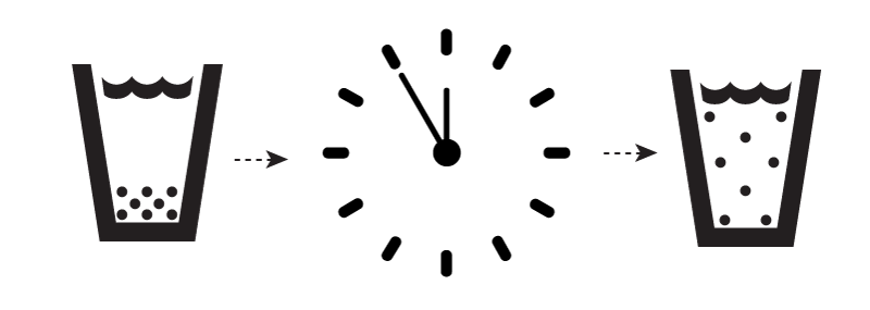
In energy, there is one feature, it always seeks to be the minimum possible in any situation. This is a law of nature. In a way, everything that happens around us can be explained precisely by this law. It is sometimes called the principle of least energy. Actually, therefore, after the jump, we always fall down, the coffee always cools down, the wind blows somewhere, etc. The same principle explains the phenomenon of diffusion. For a visual representation, you can see what happens if you put a piece of sugar in a glass with water and do not stir it.

After dissolving, the sugar particles will be in one place, for example, at the bottom of the glass. After some time, it will be noticed that all the water in the glass has become sweet, i.e. sugar particles are placed completely over the entire volume of the glass. This is shown schematically in the figure below.
This is the behavior of particles of a substance called diffusion. Therefore, it can be said that since all objects consist of molecules and atoms, then in the presence of a region where there are more particles (molecules or atoms) than in other regions, a transfer from a region of higher concentration to a smaller one occurs. In other words, nature seeks to equalize everything in order to minimize energy, lead to a state of equilibrium (sometimes they say to an equilibrium state).
Summary
Due to the laws of nature, particles of a substance, if there are a lot of them somewhere, will always strive to where they are few. This phenomenon is called diffusion.
Step 3. Solids
The idea of how the various materials are arranged is very, very difficult. There are various directions in physics, which study certain issues related to substances. For the understanding of semiconductor electronics, solids are of primary interest. Various subtleties of this issue can be studied in textbooks on solid state physics or materials science. The main (surface) idea is that all solids can be represented in the form of lattices. These are certain structures that are composed of atoms. The picture below shows some types of lattice models. The black dots in the figure are atoms.

The properties of various materials are determined by the types of their lattices, the types of atoms, and a number of other factors. Any reasoning about the structure of matter will ultimately lead to questions of quantum physics with its “magical” phenomena.
The band theory of a rigid body is well suited for describing the "entrails" of materials. This theory is inextricably linked with the concept of energy. We have already mentioned the specificity of the term “energy”. Here and in the future we will not deepen this concept. You can learn about the role that energy plays from an ordinary model of the atom by looking at the figure below.
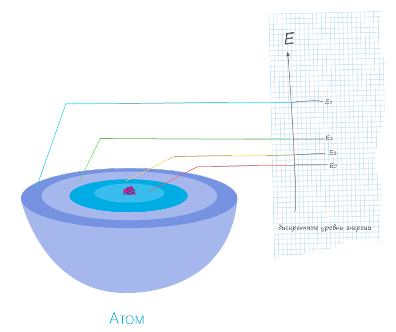
The picture shows a rough model of an atom in the form of a layered structure. In the center is the nucleus of the atom, which is surrounded by electron clouds. Electron clouds are electrons themselves. Such a representation of an electron is more like the truth than a representation in the form of balls from the point of view of quantum physics. The electronic layer is also called the electronic level. The fact is that at each level electrons have some kind of energy. The “farther” from the core - the more energy. It is also convenient to depict such a structure in the form of an energy diagram, which is also shown in the figure above. Such a diagram can often be found in textbooks on physics. Energy is denoted by the letter E. The highest energy level is called valence.
When the atoms are "connected" with each other, forming a lattice, i.e. they form some body (material), their energy levels change due to the fact that atoms act on each other. And among the energy levels there is a certain order: the energy levels are divided into so-called zones. Hence the name - zone theory. The figure below shows possible cases of zone distribution. It should be noted that these are characteristics of the entire material.

The lower zone is called the valence band. The electrons that are there are atoms. The electrons that are in the upper zone are “common”. These electrons react very well to the electric field and are directly responsible for the formation of an electric current in a substance, i.e. for its electrical properties. This zone is called the conduction band. Between them there is a forbidden zone. The picture also shows how the properties of materials and belonging to one or another class of substances depend on the width of the forbidden zone. It can be seen that the zones of the metal overlap, so they have electrons easily become “common” and, accordingly, there is a lot of them in the conduction band and a good appreciable current flows. In semiconductors, the zones are located at some distance, but not significant. This means that an electron can “jump over” through this zone if it receives enough energy from outside. Dielectrics have a wider zone, therefore it is difficult to “throw” electrons into the conduction band, as a result of which very small currents flow there. And generally they say that dielectrics do not conduct currents.
There are a number of other equally important points, but here their consideration will be omitted and for an initial understanding of the essence of physical nature, this data will suffice.
Summary
To describe the properties of solids, zone theory is used. The essence of the theory is that there are electrons inside the material that can participate in the formation of electric current, while the rest belong to atoms. If energy (light, heat, electric field) is supplied to the material, then it is possible to “tear” electrons from the atom so that they conduct current. There are materials where it is easy to do, and there is where it is difficult. "Golden mean" is a class of materials - semiconductors. In fact, all the properties of substances are described by quantum physics.
Step 4. Semiconductors
What is so special about semiconductor materials that they made a revolution in technology? The whole secret lies precisely in a fairly narrow forbidden zone. Giving electrons any energy, you can adjust the conductivity of the material. It may be
electric field, light (electromagnetic waves), temperature, etc. This explains the enormously widespread use of semiconductor devices.
For more detailed consideration, you should introduce some terms used in theory. First of all "holes". The point is this. If an electron "flies away" from the valence band, then there will be free space. Another electron can "fly" to this place. Because the electron has a negative electric charge, then “flying away” from the atom, it carries away this piece of the total charge of the atom and the atom becomes a bit more positive. Of course, the reasoning is rude, but it suggests that it is possible to imagine that a hole has formed at the site of the electron, which “carries” a positive charge. This is such a good idea that in the theory of semiconductors, these "holes" are even called particles. Although in reality this is not a particle at all, but just such a trick. This trick is convenient for the theory, so we will not dwell on this in detail, but we will use this terminology. Also, "holes" and electrons in the theory of semiconductors are called p and n particles from positive and negative, respectively.
Now, with the new terminology, we can say that when energy is supplied to the semiconductor, which is enough to “jump” the electron, a pair p and n is formed. At temperatures above 0 Kelvin (this is in human units -273 Celsius) there is always some amount of energy that is supplied to the semiconductor due to temperature. Therefore, if we take any piece of semiconductor, then we can say with full confidence that pairs of p and n particles are constantly generated and disappear (recombine) in it. This process goes on constantly and in such material there is always some amount of electrons and holes that have already been created, but have not yet had time to recombine. Their number is the same, since they are formed in pairs. But this is not enough. In order to use semiconductors for practical purposes, create special materials with parameters that are known to be set. In this case, some additional substance is introduced into the pure semiconductor, which increases either the number of electrons or "holes". Such semiconductors are called impurity (because something was mixed into them). Some are called n-type semiconductors, others are p-types. We will not touch the physical details, you can read about it in the additional literature.
Once in semiconductors there are two types of particles with a charge that can move in an orderly manner, then there are two types of current in semiconductors: electron and hole. In addition, these particles can move either due to an electric field or due to diffusion. Accordingly, the currents can still be either diffusion or drift.
The most popular semiconductor materials at the moment are silicon , germanium and gallium arsenide compound.
The complex and most important design in semiconductor applications is the contact of p-type and n-type semiconductors, the so-called pn junction.
Summary
Semiconductor materials have a relatively narrow band gap, which makes them flexible in electrical applications. In the terminology of the theory, the concept of "hole" is used, which is interpreted as a particle and can create electric current. "Hole" is free space under the electron and "has" a positive charge. In a pure semiconductor, an equal number of electrons and "holes." For technical applications, create special materials with a large number of either "holes" (p-type) or electrons (n-type).
Step 5. PN Transition
If you take two semiconductor materials and connect them as shown in the figure below, you can get a pn junction. In fact, they do not do this, because it is impossible to obtain a common crystal lattice simply by attaching two materials, but for general concepts such a model is sufficient.

Let me remind you that an impurity was added to a pure semiconductor, thanks to which the material began to have an increased concentration of charges, in one case “holes”, in the other - electrons.
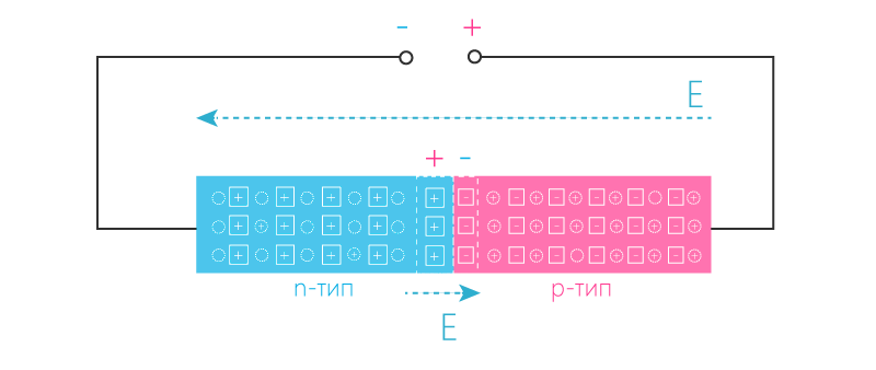
As soon as the two materials are "connected", forming a single piece of substance, the phenomenon of diffusion occurs, which tends to equalize the concentration of particles throughout the volume. The most interesting thing here will occur at the border, where electrons and holes are recombined (destroyed). Ultimately, a thin layer without “holes” and electrons will appear near the boundary of the two materials, i.e. the whole charge was compensated. However, the impurities that have been added to the materials contribute to this. These impurities are ions (atoms) that also have some kind of charge. This layer is shown in the figure.

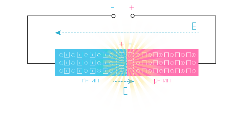
The fact that there are charged ions, and prevents further growth of the layer of recombined pairs of electrons and "holes". The fact is that between two oppositely charged areas an electric field is formed, the intensity of which is directed from the positive to the negative. As a result, an equilibrium arises in the material: at a certain layer thickness, the field will be so strong as to send back charged particles (p and n) that will tend to flow under the action of diffusion into another region. The confrontation of the electric field and diffusion and form a pn junction. The figure below shows it more clearly.

In the figure, the squares are ions, and the circles are particles (p and n). It should be noted that if the n-type conductor does not mean that there are only electrons there, there are also holes there, but there are very few of them. This can be seen in the diagram, which is drawn on a piece of paper. One can guess that for those particles that are few in a particular area, the field will accelerate them, i.e. miss. This is the so-called current of minority charge carriers. If the pn-junction is not touched in any way, then these currents are equal and, accordingly, the total current is zero.
The most interesting properties of a pn junction manifest themselves if it is influenced by some kind of energy, for example, electrical energy.
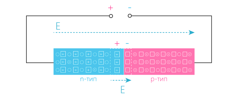
- Situation number 1. , pn-, , , , E. — . .
, .. . , . , . , , , , . , . . , , , , pn- . . , , , .
, , , . , . , . , ( ) — . , , , , , p n . « » pn-. - №2. , . . .
, , , , .. , . « » pn-. - №3. , , . , . .

— . , , pn-, -«». Because , «» , . , p n , . , , .. «» . . , pn- , , , . . , pn-, . - №4. .
, , , , , . , , , , , .. . , . , . pn- . ( ) . , , . pn-. — . .
, - , . . pn-, , , . . - .

, . . , , . , . , . pn- pn-. . , , , .
pn- , , , . , . , . , . . . , , pn-, . , , pn-.
pn- . , , , . , .
Summary
pn-, (p n). , . . , pn- .
6. -

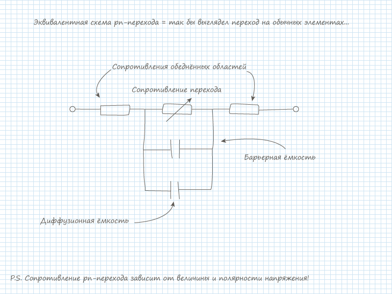
() . pn-. , . , , pn-, . .
pn- , , ( , «»). . , , .
Summary
pn- . -, pn-.
7.
. , ( ). pn-, - , . , pn- :


, . . . - , — . pn- . , . , , ( , ), pin- , , ..
. ( ) ( ), , ( ) . And much more. , pn- . .
Summary
, pn-. , pn-. .
8.
. , : .
, p, n-. . - (). , pn- () . , — , . , , . .

, : . , . . , () . . , .
pn-. pn-. pn- ( ) . , . ( ) , , ( ). . , . , , . . : () (). pn- , . , ( ) . , , ( ). . . , , .
— . (--), . ( — ). , , , , ( -, ).
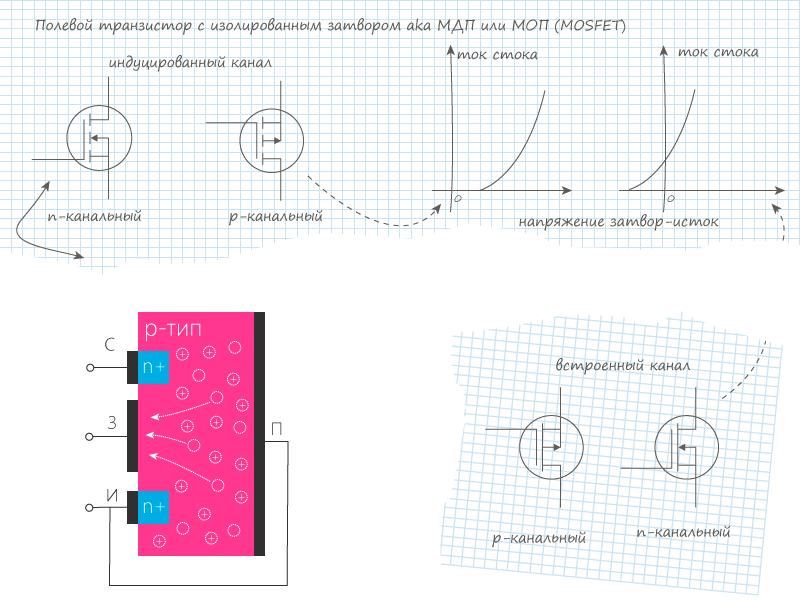
. , , , p- «» . , «» . , (). « ». , , , , - . .
, : , «» . , ( ), ( pn-).
, , (), pn- . .

: , . , . Further it will be clear why.
( ) , . . , - pn- . , , . , , , , . «» , , , . , «» . , , , .. «» «» «», . , «» n- , , . ( , ). , pn-. , .
, ( ) ( ). .

The fact is that both field and bipolar transistors can be connected to an electrical circuit in different ways, the main difference is where to send a control signal (in fact, a little differently: what output will be common for the control circuit and for the controlled one). For field-effect transistors, this description was omitted, but for bipolar, due to the significant difference, it is given for two more popular cases (it happens with a common collector).
In order not to get confused where to draw and what arrows on the designations of transistors, remember that an arrow like a compass points to N (n-type semiconductor).
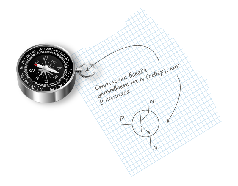
This is true for both bipolar and field-effect transistors (there can be a different type of channel). In some, it is always drawn on the emitter, in others on the gate.
In radio engineering there are many different approaches for describing devices and their parameters. One of them is a device representation in the form of a black box with several outputs. Each pin corresponds to the physical pin of the device. This approach also allows you to abstract from physics and use only the properties of the device itself. For transistors the switching circuit is typical, when one of its conclusions is common for the control circuit and for the controlled circuit. The result is that the transistor has 4 outputs. In this case, the black box is called the quadrupole. There is an obvious connection between the input and output of the device and this connection can be described by different coefficients, which are called parameters. For transistors of greatest interest are the h-parameters (H-parameters). Their values are shown in the figure below.

Among them, the most interesting is the h 21 parameter, which can often be found in the documentation for transistors, which means it will be discussed below.
The issues of working with transistors are quite complex, as with any semiconductor devices, since they also include different dependences on temperature, signal frequency, different noises, etc. We will not touch upon all of this; below we will only consider a little two probably the most popular applications of transistors, as signal amplifiers and as keys.
Summary
The most interesting device among semiconductor devices is the transistor. Transistors allow you to implement various digital and analog devices. There are two classes: bipolar (current) and field (field) transistors.
Step 9. Transistor Amplifier
When they talk about the amplifying properties of a device, they usually draw graphs, as in the figure below. The graphs show how the output changes depending on the input.
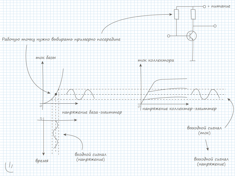
Looking at the picture, you can see the circuit; this is the simplest circuit for turning on the transistor (in this case bipolar), which allows it to amplify the signal. The most difficult thing here is to “move” the input signal in such a way (according to the input characteristic) so that it starts to amplify, and even without distortion. For this, it is necessary that the “center” of the signal be at a point from which the curve changes equally on either side. It is necessary that there is no distortion. This point is called working. For this, there is a special resistor on the circuit, which gives a constant offset to the input signal. On the graphs can be traced that the signal increased. It is seen that the amplification occurs in the current, well, and as a result of the voltage too. Therefore, to characterize the amplifying properties of transistors, special coefficients are introduced, which show how many times the output current, voltage or power is greater than the input. The parameter h 21 , discussed above, is approximately equal to the current gain. We should dwell on this, because the issues related to amplifiers and amplifier stages are complex and are generally a separate branch of electronics. Therefore, to talk about it or to say everything or nothing or almost nothing is better, only the basics are considered here. The top of perfection of semiconductor amplifiers are special cascades, which are called operational amplifiers , which now represent the whole semiconductor analog device with the most complex architecture
Summary
In analog electronics, the most popular application of transistors is an amplifier stage. Amplification occurs due to the peculiarities of the transistor. In order for the signal to be amplified without distortion, it is necessary to select the offset voltage correctly.
Step 10. Transistor Key
Another direction in the development of transistors, which has also become very popular and marked the beginning of all modern digital electronics, is the use of transistors as keys. The key is the usual switch between two states. The figure shows an example of such a conventional switch.
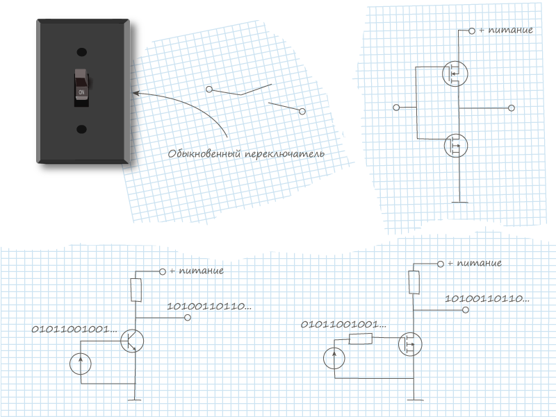
In order to make a transistor key, you must also select two states of the transistor, between which to switch. Usually this is when the transistor conducts a large current and when it is small, the transistor is said to be “open” or “closed”. From the standpoint of digital applications, this corresponds to "1" and "0". Designing digital keys also has many pitfalls and the scheme is many times more complicated than those shown in the figure, but the basis is the same. The fact is that for the keys, the switching speed as well as the distinguishability of the two states is critical. Therefore, calculations and upgrades are required in order to work optimally with the characteristics of the transistor.
The basic idea is that there is some electrical circuit with one constant resistance and one variable, which is the transistor. If the resistance of the transistor is much greater than the constant resistance, then all the voltage falls on it, and the rest on the resistor. If, however, the transistor is much less constant resistance, then the situation is the opposite. The total voltage across the transistor and the constant resistance is always equal to the supply voltage. This is the law, which is also called the Kirchhoff Law No. 2 . From here, the idea becomes clear that when a signal (current, voltage) is applied to the input of the transistor, it opens and everything falls on constant resistance, if you remove the signal, it is “closed” and everything falls on the transistor. If you measure the voltage on the transistor, then the relationship between the input and output will be similar to the logical operation inversion: when the input is “1”, the output is “0”, etc.
More popular now are the schemes, similar to the one shown in the upper right corner of the picture. This is the so-called complementary pair. Everything is simple: giving the same signal to transistors with a different type of channel, only one of the transistors will always be open. This reduces the energy consumption of the circuit.
Digital transistor keys allow you to create complex logic circuits that are already capable of performing the most complicated calculations.
Summary
In digital electronics, the most popular application of transistors is keys. Transistors switch between two states, due to which the “key” effect is manifested. Real keys are complex cascades with additional elements to improve parameters. Logic elements are formed on transistor keys.
Step 11. Logical elements
The transistor switches discussed in the previous section primarily found their use in digital electronics. You can even say that they formed it. With just one key, you can create all the necessary constructions to calculate logical functions. In mathematics it is proved that for this it is not necessary to realize all possible functions, it is enough that you can do only a few basic (basis), through which you can already express all the rest. For example, it may be an inversion operation and a conjunction (2I-He), or it may be exclusive or inversion . A simple key in itself implements the inversion. And the constructions, which are shown below in the figure, allow to realize the operation 2I-He (such a cascade is called a valve ).
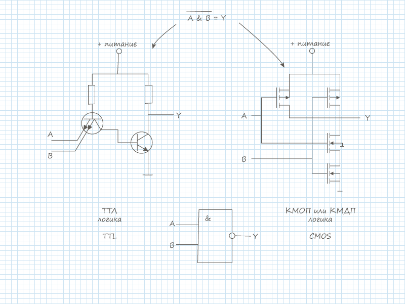
The picture shows two circuits, one for a bipolar transistor, the other for a field-effect transistor, with the field-effect transistor using complementary pairs. There are many different modifications of these types of compounds. But these are the most basic. Moreover, the CMD logic is currently the most popular, though not in its pure form. All technological innovations are a trade secret of electronics manufacturers.
Consider for example the operation of TTL (transistor-transistor logic). That interesting transistor, which is located at the input, is in fact not a specific device, it is all implemented by integrated methods, but more on that later. Let, for example, the supply voltage is 5 volts, and the inputs “A” and “B” are “0” signals, i.e. about 0.1 volts. This suggests that the emitter transitions are biased in the forward direction. If the device is made of silicon, then on such a transition there will be approximately 0.7 volts (this is a fact associated with a potential barrier). Then, relying on Kirchhoff’s Law No. 2, it can be said that between the base of the input transistor and the ground , which at the output transistor drops about 0.8 volts. Accuracy is not important here, the main thing is to understand that this is not enough, because in order for an electric current to flow through this circuit, you need at least 0.7 + 0.7, because there are two pn junctions in the circuit (one collector - from the first transistor, the second emitter - from second). Then the transistor at the output is closed, and at the output of the key "1". The situation when A and B are "1" and "0" (or "0" and "1") does not change anything, since the different potentials at the input will close, and the pn junction will also be in forward bias. However, if you submit to the input "1" and "1" ie 5 volts each, then the transitions between the base and emitters will be in reverse bias. Those. they will have small voltages, which means that the base is almost 5 volts. Here, too, accuracy is not needed. It is important that this voltage is already sufficiently and calmly open both pn junctions. This leads to the fact that the current begins to flow and the output transistor opens, the output of which is "0". This relationship between A, B, and Y is called 2I-He, since this is a logical multiplication operation and then an inversion.
Also very interesting is I2L (integrated injection logic), which is not shown here in the picture, because not very popular, but in the USSR there were significant successes in its application. Its uniqueness lies in the ultra-low power consumption (it is possible to work with voltages up to 1 volt), noise resistance and very compact dimensions (connected with planar technology). The principles of its work will not be mentioned here either, since we need to talk about many things.
Summary
Transistor switches allow to form universal logical cascades - valves that can form more complex logic functions by cascade connections. All modern digital devices consist of this kind of valves. Now, when designing microchips (about them in the next section), they rarely use a transistor scale, it all comes down to describing the connections between already-ready logic modules (often HDL languages are used for this).
Step 12. Where are the transistors in the processor?
Prominent representatives of modern semiconductor devices are processors and other chips. All these devices are built on pn-transitions. Millions of transistors form keys, which in turn form logical elements that implement various operations: addition, subtraction, multiplication, division, etc. About how on the element 2I-Not all of this can be implemented should be read in the additional literature on the algebra of logic .
Modern complex machines can “shove” such a huge number of transistors into such small sizes with the help of the so-called planar technology . Its essence is that a clean piece of semiconductor is taken (thin plate) and various levels of impurities are layered on it through a special mask to place the impurity in the right place. And so in turn forming complex compounds. These are really high technologies that do not stand still. Of course, now the operation is much more complicated than described here, but the principle remains the same. More information about the production of semiconductor chips can be found in the literature, as well as see interesting articles from Intel .

Summary
This article briefly (where possible) talks about a very important area of electronics. The topics considered can indeed be considered the most crucial for a general understanding of the principles of functioning of semiconductor devices. Find the answers to the questions that will help list of books and articles below. Of course, the semiconductor electronics industry for a long time will set the pace of scientific and technical development of society. Not without reason, processors, as representatives of this trend, have been included in the technology trends of 2012 according to the EE Times .
Step 13. Read
- Kittel H. Introduction to solid state physics.
- Landau, L. D., Lifshits, E. M. Field Theory.
- Feynman R., Leighton R., Sands M. The Feynman Lectures on Physics. Electricity and magnetism.
- Feynman R., Leighton R., Sands M. The Feynman Lectures on Physics. Continuum Physics
- Paul Horowitz and Winfield Hill. The Art of Electronics.
- Peter Y. Yu, Manuel Cardona. Fundamentals of Semiconductors: Physics and Materials Properties.
- Li, Sheng S. Semiconductor Physical Electronics.
- S.A. Gavrilov. Semiconductor circuit. Developer Secrets.
- Tolmachev V.V., Skripnik F.V. Physical Foundations of Electronics.
- Diodes. For dummies ( AveNat ).
- Bipolar transistors. For dummies ( AveNat ).
- Field effect transistors. For dummies ( AveNat ).
- Semiconductor devices - diode ( IIIa66uMEM6eP ).
- pn junction ( Dooez ).
- The simplest logical circuit. Part 1 and Part 2 ( appplemac ).
- Autopsy Pentium III, photos under the microscope ( alizar ).
- Opening chip Nvidia 8600M GT ( Tiberius ).
PS Follow the resource rules and terms of the Creative Commons Attribution 3.0 Unported (CC BY 3.0)
Source: https://habr.com/ru/post/134373/
All Articles