Field effect transistors. For dummies
Introduction
And now let's talk about field effect transistors. What can be assumed already by their one name? First, since they are transistors, they can somehow control the output current. Secondly, they are supposed to have three contacts. And thirdly, at the heart of their work lies the pn junction. What will official sources tell us?
Field-effect transistors are active semiconductor devices, usually with three pins, in which the output current is controlled by an electric field. (electrono.ru)
The definition not only confirmed our assumptions, but also demonstrated the feature of field-effect transistors — the output current is controlled by changing the applied electric field, i.e. voltage. But in bipolar transistors , as we remember, the output current is controlled by the input base current.
Another fact about field effect transistors can be found by drawing attention to their other name, unipolar . This means that only one type of charge carrier (or electrons, or holes) is involved in the flow of current.
The three contacts of field-effect transistors are called the source (source of current carriers), the gate (control electrode), and drain (the electrode where the carriers flow). The structure seems simple and very similar to a bipolar transistor device. But it can be implemented in at least two ways. Therefore, field-effect transistors with a control pn junction and with an isolated gate are distinguished.
')
In general, the idea of the latter appeared in the 20s of the 20th century, long before the invention of bipolar transistors. But the level of technology allowed to implement it only in 1960. In the 50s, it was first theoretically described, and then the field effect transistor with a control pn junction was implemented. And, like their bipolar "brothers", field-effect transistors still play a huge role in electronics.
Before proceeding to the story about the physics of the work of unipolar transistors, I want to recall the links that can refresh your knowledge of the pn junction: one and two .
Field effect transistor with pn junction control

So, how does the first type of field effect transistors work? The device is based on a semiconductor plate with conductivity (for example) of p-type. At the opposite ends, it has electrodes, by applying a voltage to which we receive current from the source to the drain. On top of this plate there is an area with the opposite type of conductivity, to which the third electrode is connected - the gate. Naturally, a pn junction appears between the gate and the p-region below it (the channel ). And since the n-layer is significantly at the same channel, most of the transition region depleted of mobile charge carriers will be in the p-layer. Accordingly, if we apply a reverse bias voltage to the transition, then closing it will significantly increase the channel resistance and decrease the current between the source and drain. Thus, the output current of the transistor is regulated by the voltage (electric field) of the gate.
The following analogy can be drawn: the pn junction is a dam blocking the flow of charge carriers from the source to the drain. By increasing or decreasing the reverse voltage on it, we open / close gateways on it, adjusting the "water supply" (output current).
 So, in the operating mode of a field-effect transistor with a control pn junction, the voltage at the gate must be either zero (the channel is fully open) or reverse.
 If the magnitude of the reverse voltage becomes so large that the blocking layer closes the channel, the transistor will go into cutoff mode .
Even at zero voltage at the gate, between the gate and the drain, there is a reverse voltage equal to the source-drain voltage. That is why the pn junction has such an uneven shape, expanding towards the flow area.
It goes without saying that you can make a transistor with an n-type channel and a p-type gate. The essence of his work will not change.
 Conditional graphic images of field-effect transistors are shown in the figure ( a — with a p-type channel, b — with an n-type channel). The arrow here indicates the direction from the p-layer to the n-layer.
Static characteristics of a field-effect transistor with a control pn junction
Since, in the operating mode, the gate current is usually low or even zero, we will not consider the graphs of the input characteristics of the field-effect transistors. We turn immediately to the weekend or stock. By the way, they are called static because a constant voltage is applied to the gate. Those. there is no need to take into account frequency moments, transients, etc.

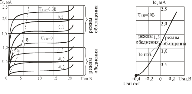
Output ( drain ) is the dependence of the drain current on the source-drain voltage at a constant gate-source voltage. The figure is a graph on the left.
The graph can clearly distinguish three zones. The first of them is the zone of sharp increase in the drain current. This is the so-called "ohmic" area . The source-drain channel behaves like a resistor whose resistance is controlled by the voltage at the gate of the transistor.
The second zone is the saturation region . It has an almost linear look. Here the channel overlaps in the drain area, which increases with a further increase in the source-drain voltage. Accordingly, the resistance of the channel grows, and the stock current changes very little (Ohm's law, however). It is this section of the characteristics used in amplifier technology, because here the least non-linear distortion of the signals and the optimal values of the small-signal parameters that are essential for amplification. Such parameters include slope, internal resistance and gain. The meanings of all these incomprehensible phrases will be explained below.
The third zone of the chart is the breakdown area , whose name speaks for itself.
On the right side of the figure shows a graph of another important relationship - the flow-gate characteristics . It shows how the drain current depends on the gate-source voltage at a constant voltage between the source and drain. And precisely its steepness is one of the main parameters of the field-effect transistor.
Insulated Gate Field Effect Transistor
Such transistors are also often called MDP (metal-dielectric-semiconductor) - or MOS (metal-oxide-semiconductor) -transistors (English metall-semiconductor field effect transistor, MOSFET). In such devices, the gate is separated from the channel by a thin layer of dielectric. The physical basis of their work is the effect of changing the conductivity of the surface layer of a semiconductor at the interface with a dielectric under the influence of a transverse electric field.
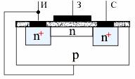 The device transistors of this type are as follows. There is a semiconductor substrate with p-conductivity, in which two heavily doped regions with n-conductivity (source and drain) are made. Between them lies a narrow near-surface jumper, the conductivity of which is also n-type. Above it on the surface of the plate there is a thin layer of dielectric (most often of silicon dioxide - hence, by the way, the abbreviation MOP). And already on this layer and the shutter is located - a thin metal film. The crystal itself is usually connected to the source, although it happens that it is connected separately.
If the source-drain voltage is applied at a zero voltage at the gate, a current will flow through the channel between them. Why not through the crystal? Because one of the pn junctions will be closed.
And now let us apply the negative voltage relative to the source to the gate. The resulting transverse electric field "push" the electrons from the channel into the substrate. Accordingly, the channel resistance will increase and the current through it will decrease. Such a mode in which the output current decreases with increasing gate voltage, is called a depletion mode .
If we apply a voltage to the gate, which will contribute to the emergence of a field “helping” the electrons to “come” into the channel from the substrate, then the transistor will work in the enrichment mode . In this case, the channel resistance will fall, and the current through it will grow.
The above construction of an insulated-gate transistor is similar to that with a control pn junction in that even at zero gate current with a non-zero source-drain voltage, there is a so-called initial drain current between them. In both cases, this is due to the fact that the channel for this current is built into the design of the transistor. That is, strictly speaking, we have just considered such a subtype of MOSFET transistors as transistors with a built-in channel .
However, there is another kind of insulated gate field effect transistors - an induced-inverse-channel transistor . From the name it is already clear that it differs from the previous one - its channel between heavily doped areas of drain and source appears only when a voltage of a certain polarity is applied to the gate.
So, we apply voltage only to the source and drain. The current between them will not flow, since one of the pn junctions between them and the substrate is closed.
Let us apply voltage to the gate (direct relative to the source). The arising electric field will “pull” electrons from heavily doped regions into the substrate in the direction of the gate. And when the voltage at the gate reaches a certain value in the near-surface zone, a so-called conduction type inversion will occur. Those. the concentration of electrons will exceed the concentration of holes, and a thin n-type channel will appear between the drain and the source. The transistor will conduct current, the stronger, the higher the voltage at the gate.
From this design, it is clear that a transistor with an induced channel can work only while in the enrichment mode. Therefore, they are often found in switching devices.
The legend of the insulated gate transistors is as follows:

Here
a - with built-in n-type channel;
b - with built-in p-type channel;
in - with a conclusion from a substrate;
d - with an induced n-type channel;
d - with induced p-type channel;
e - with output from the substrate.
Static characteristics of MOSFETs
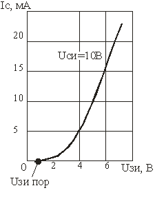
The family of stock and drain-gate characteristics of the transistor with a built-in channel are shown in the following figure:
The same characteristics for a transistor with an induced channel:

Exotic MDP-structures
In order not to confuse the presentation, I just want to advise links on which you can read about them. First of all, this is everyone’s beloved Wikipedia , section “Special-purpose TIR structures”. And here is the theory and formulas: a textbook on solid-state electronics, Chapter 6 , subchapters 6.12-6.15. Read it, it's interesting!
General parameters of field-effect transistors
- Maximum drain current at a fixed gate-source voltage.
- The maximum drain-source voltage , after which the breakdown already occurs.
- Internal (output) resistance . It is the channel resistance for alternating current (gate-source voltage is constant).
- The steepness of the slide-bolt characteristics . The larger it is, the sharper the transistor's response to a change in voltage at the gate is.
- Input impedance . It is determined by the resistance of the reverse biased pn junction and usually reaches units and tens of MOhm (which distinguishes field-effect transistors from bipolar "relatives"). And among the field-effect transistors, the palm belongs to devices with an insulated gate.
- Gain is the ratio of the source-drain voltage change to the gate-source voltage change at a constant drain current.
Inclusion schemes

As a bipolar field-effect transistor can be considered as a quadrupole, in which two of the four contacts are the same. Thus, it is possible to distinguish three types of switching circuits: with a common source, with a common gate and with a common drain. According to the characteristics, they are very similar to the schemes with a common emitter, a common base and a common collector for bipolar transistors.
The most commonly used scheme with a common source ( a ), as giving greater gain in current and power.
The common gate circuit ( b ) almost no current amplification and has a small input resistance. Because of this, such an inclusion scheme has limited practical application.
The circuit with a common drain ( c ) is also called a source follower . Its voltage gain is close to unity, the input resistance is large, and the output is small.
Differences field transistors from bipolar. Areas of use
As mentioned above, the first and most important difference between these two types of transistors is that the latter are controlled by changing the current, and the former are controlled by voltages. And from this follow the other advantages of field-effect transistors in comparison with bipolar ones:
- high input impedance at a constant current and at a high frequency, hence the small loss of control;
- high speed (due to the absence of accumulation and resorption of minority carriers);
- since the amplifying properties of field-effect transistors are due to the transfer of the main charge carriers, their upper limit of the effective gain is higher than that of bipolar ones;
- high temperature stability;
- low noise level, since the field-effect transistors do not use the phenomenon of injection of minority charge carriers, which makes bipolar transistors "noisy";
- low power consumption.
However, in this case, field-effect transistors have a disadvantage - they “fear” static electricity, therefore, when working with them, they place particularly stringent requirements on protection against this scourge.
Where are field-effect transistors used? Yes, almost everywhere. Digital and analog integrated circuits, tracking and logic devices, energy-saving circuits, flash memory ... Yes, there, even a quartz watch and a TV remote control work on field-effect transistors. They are everywhere,% habraiser %. But now you know how they work!
List of sources:
ru.wikipedia.org
dssp.petrsu.ru
zpostbox.narod.ru
electrono.ru
radio.cybernet.name
Useful comments:
http://habrahabr.ru/blogs/easyelectronics/133493/#comment_4435883
http://habrahabr.ru/blogs/easyelectronics/133493/#comment_4436509
http://habrahabr.ru/blogs/easyelectronics/133493/#comment_4441531
I recommend to read:
"Basics on the fingers," by DI HALT (thanks to AlexeiKozlov for the tip)
Source: https://habr.com/ru/post/133493/
All Articles