Bipolar transistors. For dummies
Foreword
Since the topic of transistors is very and very extensive, there will be two articles devoted to them: separately on bipolar and separately on field-effect transistors.
The transistor, like the diode, is based on the phenomenon of the pn junction. Those who wish can refresh the memory of the processes occurring in it here or here .
The necessary explanations are given, go to the point.
Transistors. Definition and history
The transistor is an electronic semiconductor device in which the current in the circuit of two electrodes is controlled by a third electrode. (tranzistors.ru)
The first field-effect transistors were invented (1928), and bipolar appeared in 1947 in the Bell Labs laboratory. And it was, without exaggeration, a revolution in electronics.
')
Very quickly, transistors replaced vacuum tubes in various electronic devices. In this regard, the reliability of such devices has increased and their size has decreased significantly. And to this day, no matter how “tricked” the microcircuit is, it still contains many transistors (as well as diodes, capacitors, resistors, etc.). Only very small.
By the way, initially “transistors” called resistors, the resistance of which could be changed using the magnitude of the supplied voltage. If we ignore the physics of processes, then a modern transistor can also be represented as a resistance depending on the signal applied to it.
What is the difference between field and bipolar transistors? The answer lies in their very names. In a bipolar transistor, both electrons and holes are involved in charge transfer ("bis" - twice). And in the field (he is unipolar) - or electrons, or holes.
Also, these types of transistors vary by application. Bipolar are mainly used in analog technology, and field - in digital.
And finally: the main area of application of any transistors is the amplification of a weak signal due to an additional power source.
Bipolar transistor. Principle of operation. Main characteristics
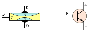
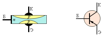
The bipolar transistor consists of three areas: the emitter, the base and the collector, each of which is energized. Depending on the type of conductivity of these areas, npn and pnp transistors are isolated. Usually the collector area is wider than the emitter. The base is made of a lightly doped semiconductor (which is why it has great resistance) and is made very thin. Since the emitter-base contact area turns out to be much smaller than the base-collector contact area, it is impossible to change the emitter and collector places by changing the polarity of the connection. Thus, the transistor refers to unbalanced devices.
Before considering the physics of the transistor, we outline the general problem.
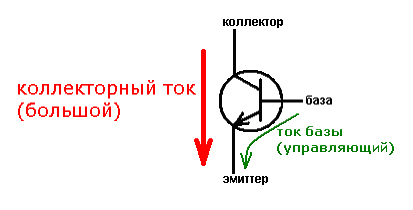
It consists in the following: a strong current flows between the emitter and a collector ( collector current ), and a weak control current ( base current ) flows between the emitter and the base. The collector current will change depending on the change in the base current. Why?
Consider the pn junction transistor. There are two of them: emitter base (EB) and base-collector (BC). In the active mode of the transistor, the first of them is connected with a direct one, and the second with a reverse bias. What happens at the same time on pn junctions? For greater certainty, we will consider the npn transistor. For pnp, everything is the same, only the word “electrons” must be replaced with “holes”.
Since the EB transition is open, the electrons easily “run across” into the base. There, they partially recombine with holes, but most of them, due to the small thickness of the base and its weak doping, have time to reach the base-collector transition. Which, as we recall, is included with reverse bias. And since electrons in the base are minor charge carriers, the electric field of the transition helps them overcome it. Thus, the collet current is only slightly less than the emitter current. And now watch your hands. If you increase the base current, then the transition of the EB will open up stronger, and between the emitter and the collector will be able to slip more electrons. And since the collector current is initially greater than the base current, this change will be very, very noticeable. Thus, there will be an increase in the weak signal received at the base . Once again: a strong change in the collector current is proportional to the reflection of a weak change in the base current.
I remember that my one-to-one principle of operation of the bipolar transistor was explained on the example of a water tap. The water in it is the collector current, and the control current of the base is how far we turn the knob. Enough small effort (control) to increase the flow of water from the tap.
In addition to the considered processes, a number of phenomena may occur on the pn junctions of the transistor. For example, with a strong increase in voltage at the base-collector junction, avalanche charge multiplication may begin due to impact ionization. And coupled with the tunnel effect, this will give first electric, and then (with increasing current) and thermal breakdown. However, thermal breakdown in the transistor can occur without electric current (i.e., without raising the collector voltage to the breakdown voltage). For this, one overcurrent through the collector will suffice.
Another phenomenon is due to the fact that when the voltages at the collector and emitter junctions change, their thickness changes. And if the base is too thin, there may be a closure effect (the so-called “puncture” of the base) - a connection of the collector junction with the emitter. In this case, the base region disappears, and the transistor stops working normally.
The collector current of the transistor in the normal active mode of the transistor is greater than the base current a certain number of times. This number is called the current gain and is one of the main parameters of the transistor. It is denoted by h21 . If the transistor is turned on without a load on the collector, then at a constant collector-emitter voltage, the ratio of the collector current to the base current will give a static current gain . It can be equal to tens or hundreds of units, but it is worth considering the fact that in real circuits this coefficient is less due to the fact that when the load is turned on, the collector current naturally decreases.
The second important parameter is the input impedance of the transistor . According to Ohm’s law, it is the ratio of the voltage between the base and the emitter to the control current of the base. The larger it is, the lower the base current and the higher the gain.
The third parameter of the bipolar transistor is the voltage gain . It is equal to the ratio of the amplitude or effective values of the output (emitter-collector) and input (base-emitter) of alternating voltages. Since the first value is usually very large (units and tens of volts), and the second is very small (tenths of volts), this coefficient can reach tens of thousands of units. It is worth noting that each base control signal has its own voltage gain.
Also, transistors have a frequency response that characterizes the transistor's ability to amplify a signal, the frequency of which approaches the edge frequency of the gain. The fact is that with an increase in the frequency of the input signal, the gain decreases. This is due to the fact that the flow time of the main physical processes (the time of carrier transfer from the emitter to the collector, the charge and discharge of barrier capacitive transitions) becomes comparable with the period of change of the input signal. Those. the transistor simply does not have time to react to changes in the input signal and at some point simply ceases to amplify it. The frequency at which this occurs is called the limiting one .
Also the parameters of the bipolar transistor are:
- reverse current collector-emitter
- on time
- reverse current collector
- maximum allowed current
Legend npn and pnp transistors differ only in the direction of the arrow designating the emitter. It shows how current flows in a given transistor.
Modes of operation of the bipolar transistor
The above option is a normal active mode of the transistor. However, there are several more combinations of openness / closeness of pn junctions, each of which represents a separate mode of operation of the transistor.
- Inverse active mode . Here the BC transition is open, and the EB is closed on the contrary. Naturally, amplification properties in this mode are worse than ever, therefore transistors in this mode are used very rarely.
- Saturation mode . Both transitions are open. Accordingly, the main charge carriers of the collector and emitter “run” into the base, where they actively recombine with its main carriers. Due to the excess charge carriers, the base resistance and pn junctions decrease. Therefore, the circuit containing the transistor in the saturation mode can be considered short-circuited, and the radio element itself can be represented as an equipotential point.
- Cutoff mode . Both transitions of the transistor are closed, i.e. The main charge carrier current between the emitter and the collector is terminated. Flows of minority carriers create only small and uncontrollable thermal currents of transitions. Due to the poverty of the base and carrier transitions, their resistance increases greatly. Therefore, it is often considered that the cut-off transistor is an open circuit.
- Barrier mode In this mode, the base is directly or through low resistance closed with a collector. Also in the collector or emitter circuit include a resistor that sets the current through the transistor. Thus, the equivalent of a diode circuit with a series-connected resistance is obtained. This mode is very useful, as it allows the circuit to work at almost any frequency, in a large temperature range and is undemanding to the parameters of transistors.
Bipolar Transistor Power Circuits
Since the transistor has three contacts, in general, it must be powered from two sources, which together make four leads. Therefore, one of the contacts of the transistor has to be energized with the same sign from both sources. And depending on what kind of contact, there are three switching circuits for bipolar transistors: with a common emitter (MA), a common collector (OK) and a common base (ON). Each of them has both advantages and disadvantages. The choice between them is made depending on which parameters are important for us and which ones we can sacrifice.
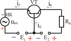
Inclusion scheme with a common emitter
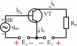
This scheme gives the greatest gain in voltage and current (and hence in power - up to tens of thousands of units), and therefore is the most common. Here, the emitter-base transition is switched on directly, and the base-collector transition is turned back. And since both the base and the collector are energized with the same sign, the circuit can be powered from one source. In this scheme, the phase of the output AC voltage varies with respect to the phase of the input AC voltage by 180 degrees.
But to all the buns, the scheme with OE has a significant drawback. It lies in the fact that the increase in frequency and temperature leads to a significant deterioration of the amplifying properties of the transistor. Thus, if the transistor should operate at high frequencies, then it is better to use another switching circuit. For example, with a common base.
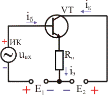
Common base wiring diagram
This scheme does not give a significant signal gain, but is good at high frequencies, since it allows more full use of the frequency response of the transistor. If the same transistor is switched on first according to the scheme with a common emitter, and then with a common base, then in the second case a significant increase in its edge amplification frequency will be observed. Since with such a connection the input impedance is low and the output impedance is not very large, the cascades of transistors assembled according to the OUT circuit are used in antenna amplifiers, where the characteristic impedance of cables usually does not exceed 100 Ohms.
In the scheme with a common base, the phase of the signal does not invert, and the level of noise at high frequencies decreases. But, as already mentioned, the current gain is always a little less than one. True, the voltage gain is the same here as in the circuit with a common emitter. The disadvantages of the scheme with a common base can also be attributed to the need to use two power sources.
Common collector wiring diagram
The peculiarity of this circuit is that the input voltage is completely transferred back to the input, that is, negative feedback is very strong.
Let me remind you that negative is called such feedback, in which the output signal is fed back to the input, which reduces the level of the input signal. Thus, an automatic adjustment occurs when a random change in the parameters of the input signal
The current gain is almost the same as in the common emitter circuit. But the voltage gain is small (the main disadvantage of this circuit). It is close to one, but always smaller. Thus, the gain in power is equal to only a few dozen units.
In the circuit with a common collector, there is no phase shift between the input and output voltage. Since the voltage gain is close to unity, the output voltage in phase and amplitude coincides with the input voltage, i.e. it repeats it. That is why this scheme is called an emitter follower. Emitter - because the output voltage is removed from the emitter relative to the common wire.
Such an inclusion is used to match the transistor stages or when the input source has a high input impedance (for example, a piezoelectric pickup or a condenser microphone).
Two words about cascades
It happens that you need to increase the output power (ie, increase the collector current). In this case, use the parallel connection of the required number of transistors.
Naturally, they should be about the same in characteristics. But it must be remembered that the maximum total collector current should not exceed 1.6-1.7 of the limit current of the collector of any of the transistors of the cascade.
Nevertheless (thanks to wrewolf for the remark), in the case of bipolar transistors, this is not recommended. Because two transistors of even one tipominal slightly, but differ from each other. Accordingly, with parallel connection, currents of different size will flow through them. To align these currents in the emitter circuit of the transistors put balanced resistors. The magnitude of their resistance is calculated so that the voltage drop on them in the range of operating currents was not less than 0.7 V. It is clear that this leads to a significant deterioration in the efficiency of the circuit.
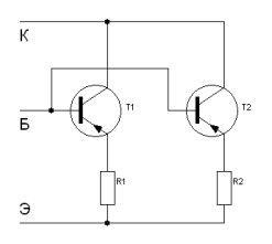
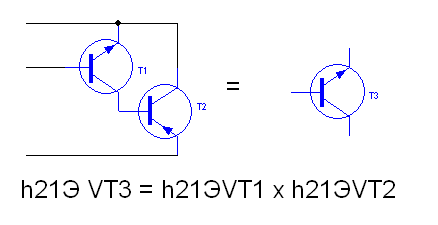
It may also be necessary to have a transistor with good sensitivity and with a good gain. In such cases, a cascade of a sensitive, but low-power transistor (in the figure - VT1) is used, which controls the power supply of a more powerful fellow (in the figure - VT2).
Other Bipolar Transistor Applications
Transistors can be used not only to amplify the signal. For example, due to the fact that they can operate in saturation and cutoff modes, they are used as electronic keys. It is also possible to use transistors in signal generator circuits. If they work in the key mode, a square wave will be generated, and if in the gain mode, then an arbitrary waveform is dependent on the control action.
Marking
Since the article has already grown to an indecently large volume, at this point I will simply give two good links, which describe in detail the main marking systems of semiconductor devices (including transistors): http://kazus.ru/guide/transistors/mark_all .html and .xls file (35 kb) .
List of sources:
http://ru.wikipedia.org
http://www.physics.ru
http://radiocon-net.narod.ru
http://radio.cybernet.name
http://dvo.sut.ru
Useful comments:
http://habrahabr.ru/blogs/easyelectronics/133136/#comment_4419173
Source: https://habr.com/ru/post/133136/
All Articles