Diodes. For dummies
Introduction
The diode is a two-electrode electronic device, it has different conductivity depending on the direction of the electric current. The diode electrode connected to the positive pole of the current source when the diode is open (that is, it has a small resistance) is called the anode, which is connected to the negative pole — the cathode. (wikipedia)
All diodes can be divided into two large groups: semiconductor and non-semiconductor. Here I will consider only the first one.
The basis of a semiconductor diode is such a famous thing as the pn junction. I think that most of the readers were told about him at the physics lessons at school, and to others in more detail at the institute. However, just in case, I will give a general principle of its work.
Two words about the band theory of the conductivity of solids
Before you start talking about the pn transition, it is worth discussing some theoretical points.
It is believed that the electrons in an atom are located at different distances from the nucleus. Accordingly, the closer the electron is to the nucleus, the stronger the connection between them and the more energy must be applied in order to send it “in free navigation”. It is said that electrons are located at different energy levels . The filling of these levels with electrons occurs from the bottom up, and on each of them there can be no more than a strictly defined number of electrons ( Bohr atom ). Thus, if the level is filled, then a new electron cannot reach it until a place is made available for it. In order for an electron to go one level higher, it needs to communicate additional energy. And if the electron "falls" down, then the excess energy is released in the form of radiation. Electrons can occupy only highly defined orbits with certain energies in an atom. These orbits are called allowed . Accordingly, forbidden are those orbits (zones) in which an electron cannot be. You can read more about this by referring to the Bohr atom above, but here we take it as an axiom.
')
The highest energy level is called the valence . For most substances, it is only partially filled, so the electrons of the outer sublevels of other atoms can always find a place on it. And they really randomly migrate from atom to atom, thus making the connection between them. The bottom layer in which free electrons can move is called the conduction band . If the valence band is partially filled and the electrons in it can move from atom to atom, then it coincides with the conduction band. This picture is observed in conductors. In semiconductors, the valence band is completely filled, but the energy difference between the valence and conducting levels of them is small. Therefore, electrons can overcome it simply by thermal motion. And in insulators, this difference is large, and in order to get a breakdown, you need to apply considerable energy.
This is the general picture of the energy structure of the atom. You can go directly to the pn junction.
pn junction
To begin with, semiconductors are n-type and p-type. The former are obtained by doping a tetravalent semiconductor (most often silicon) with a pentavalent semiconductor (for example, arsenic). This pentavalent impurity is called a donor . Its atoms form four chemical bonds with silicon atoms, and the fifth valence electron remains free and can escape from the valence band to the conduction band, if, for example, the temperature of the substance is slightly increased. Thus, in the n-type conductor an excess of electrons occurs.
P-type semiconductors are also obtained by doping silicon, but by a trivalent impurity (for example, boron). This impurity is called the acceptor . It can form only three of the four possible chemical bonds. And the remaining unfilled valence bond is called a hole . Those. a hole is not a real particle, but an abstraction adopted for a more convenient description of the processes occurring in a semiconductor. Its charge is considered positive and equal to the charge of the electron. So, in a p-type semiconductor, we get an excess of positive charges.
In both types of semiconductors, in addition to the main charge carriers (electrons for the n-type, holes for the p-type), minority carriers are present in large quantities: holes for the n-region and electrons for the p-region.

If p-and n-semiconductors are located next to each other, a diffuse current will appear at the boundary between them. This will happen because, on the one hand, we have too many negative charges (electrons), and on the other, positive (holes). Accordingly, the electrons will flow into the border region of the p-semiconductor. And since a hole is a place where there is no electron, there will be a feeling that the holes are moving in the opposite direction - towards the boundary of the n-semiconductor. Getting into the p- and n-regions, electrons and holes recombine, which leads to a decrease in the number of mobile charge carriers. Against this background, immovable positively and negatively charged ions at the boundaries of semiconductors (from which recombined holes and electrons are gone) are clearly visible. As a result, we obtain two narrow charged regions at the boundary of substances. This is the pn junction, which is also called the depleted layer due to the low concentration of mobile charge carriers in it. Naturally, an electric field will arise here, the direction of which prevents further diffusion of electrons and holes. A potential barrier arises, which the main charge carriers can overcome only if they possess enough energy for that. On the contrary, the arising electric field helps minor carriers. Accordingly, a current will flow through the junction in the opposite diffuse direction. This current is called drift . In the absence of external influence, the diffuse and drift currents balance each other and the flow of charges ceases.
The width of the depleted region and the contact potential difference of the transition boundaries (potential barrier) are important characteristics of the pn junction.
If an external voltage is applied so that its electric field “maintains” the diffuse current, then the potential barrier will decrease and the depletion region will become narrow. Accordingly, the current will be easier to flow through the junction. Such an external voltage connection is called forward bias.
But you can connect and vice versa, so that the external electric field supports the drift current. However, in this case, the width of the depleted zone will increase, and the potential barrier will increase. The transition "closes." Such a connection is called reverse bias. If the magnitude of the applied voltage exceeds a certain limit value, a breakdown of the transition will occur, and a current will flow through it (the electrons will accelerate to such an extent that they can slip through the potential barrier). This limit value is called the breakdown voltage.
Everything, the end of the theory, it's time to move on to its practical application.
Diodes, finally

Diode, in fact, a single pn junction. If it is connected with forward bias, then the current flows through it, and if with a reverse one it does not flow (in fact, a small drift current still remains, but this can be neglected). This principle is shown in the symbol of the diode: if the current is directed along the arrow of the triangle, then nothing interferes with it, and if vice versa, then it “bumps” into a vertical line. This vertical line on the diodes of radio elements is indicated by a wide band at the edge.
I remember when I was a stupid student and first came to work in the shop for printing printed circuit boards, I first put diodes on like a god for the soul. Only then I learned that the correct location of this element plays a very, very significant role. But this is so, a lyrical digression.
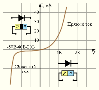
Diodes have a non-linear current-voltage characteristic.
Diode application areas
- Straightening alternating current. It is based precisely on the property of the "lock" diode with reverse bias. Diode as it "cuts" the negative half-waves.
- As variable capacity. These diodes are called varicaps .

Here, the dependence of the barrier capacitance of the transition on the reverse bias is used. The greater its value, the wider the depleted area of the pn junction. It can be imagined as a flat capacitor, the plates of which form the boundaries of the region, and it acts as a dielectric. Accordingly, the thicker the “dielectric layer”, the lower the barrier capacitance. Therefore, by varying the applied voltage, it is possible to electrically change the capacity of varicap. - To stabilize the voltage. The principle of operation of such diodes is that even with a significant increase in the external voltage drop, the voltage drop across the diode will increase slightly. This is true for both forward and reverse bias. However, the breakdown voltage at reverse bias is much higher than the forward voltage of the diode. Thus, if you need to maintain a high voltage stable, it is better to turn the diode back on. And to keep it working, despite the breakdown, you need to use a special type of diode - a zener diode .

In straight mode, it will work like a normal rectifying diode. But in the reverse-biased it will not conduct current until the applied voltage reaches the so-called voltage of the Zener diode, at which the diode will be able to conduct significant current, and the voltage will be limited by the voltage level of the Zener diode. - As a "key" (switching device). Such diodes should be able to open and close very quickly depending on the applied voltage.
- As radiation detectors ( photodiodes ).

Light quanta transfer additional energy to atoms in the n-region, which leads to the appearance of a large number of new electron-hole pairs. When they reach the pn junction, the holes go into the p-region, and the electrons accumulate at the edge of the junction. Thus, there is an increase in the drift current, and between the p- and n-regions there is a potential difference, called photo-emf. Its magnitude is greater, the greater the luminous flux. - To create optical radiation ( LEDs ).

During the recombination of holes and electrons (forward bias), the transition of the latter to a lower energy level occurs. "Excess" energy is released in the form of a quantum of energy. And depending on the chemical composition and properties of a semiconductor, it emits waves of a particular range. The radiation efficiency also depends on the composition.
A bit of exotic
Do not forget that the pn transition is one of the phenomena of the microworld where quantum physics rules the ball and strange things become possible. For example, the tunnel effect - when a particle can pass through a potential barrier, with less energy. This becomes possible due to the uncertainty of the relationship between the momentum and the coordinates of the particle (hello, Heisenberg!). This effect underlies the tunnel diodes .

To ensure the possibility of "leakage" of charges, they are made of degenerate semiconductors (containing a high concentration of impurities). The result is a sharp pn junction with a thin barrier layer. Such diodes are low-power and low-inertia, so they can be used in the microwave range.
There is another unusual type of semiconductor diodes - Schottky diodes .

They use not the traditional pn junction, but the metal-semiconductor junction as a Schottky barrier. This barrier arises in the case when the magnitudes of the work function of electrons from a metal and a semiconductor differ. If the n-semiconductor has a work function less than the metal in contact with it, then the boundary metal layer will be negatively charged, and the semiconductor will be positive (it is easier for electrons to transfer from the semiconductor to the metal than vice versa). If we have a metal / p-semiconductor contact, and the work function for the second is higher than for the first, then we get a positively charged boundary layer of metal and a negatively charged layer of semiconductor. In any case, we will have a potential difference with which the work functions of both contacting substances will be equal. This will lead to the emergence of an equilibrium state and the formation of a potential barrier between the metal and the semiconductor. And just as in the case of the pn junction, a forward and reverse bias can be applied to the metal / semiconductor junction with a similar result.
Schottky diodes differ from their pn counterparts by low voltage drops with direct switching on and a smaller electrical capacitance of the junction. Thus, their operating frequency increases and the level of interference decreases.
Conclusion
Of course, not all existing types of diodes are considered here. But I hope that according to the above, you can make a fairly complete judgment about these electronic components.
Sources:
ru.wikipedia.org
mda21.ru
elementy.ru
femto.com.ua
Source: https://habr.com/ru/post/132842/
All Articles