An inside look: Opening the Nvidia 8600M GT chip
Foreword
About 3-4 years ago, fate decreed that the Asus G2S laptop got into my hands. My happiness lasted exactly until last winter, when, for no reason at all, artifacts began to appear on the screen, especially when launching toys or "powerful" applications that are actively working with video chips. As a result, it turned out that the problem is in it. Nvidia for almost the entire g2 gaming line delivered video chips with defects (detachment of contacts between the crystal itself and the substrate), which was detected only after a couple of years of intensive work. The solution was unequivocal - replacing the video chip. But what to do with the old? The answer to this question came extremely quickly ...
A lot of traffic under the cut
The fact is that as a “hobby,” I give lectures at the SUNTs of Moscow State University (the Kolmogorov school), and I was asked to prepare material on micro and nanoelectronics for a long time, explaining how, where and in what conditions flash drives, processors, etc. . And here such a valuable sample disappears, so that literally in a day an old video chip was under the diamond circle of the microtome .
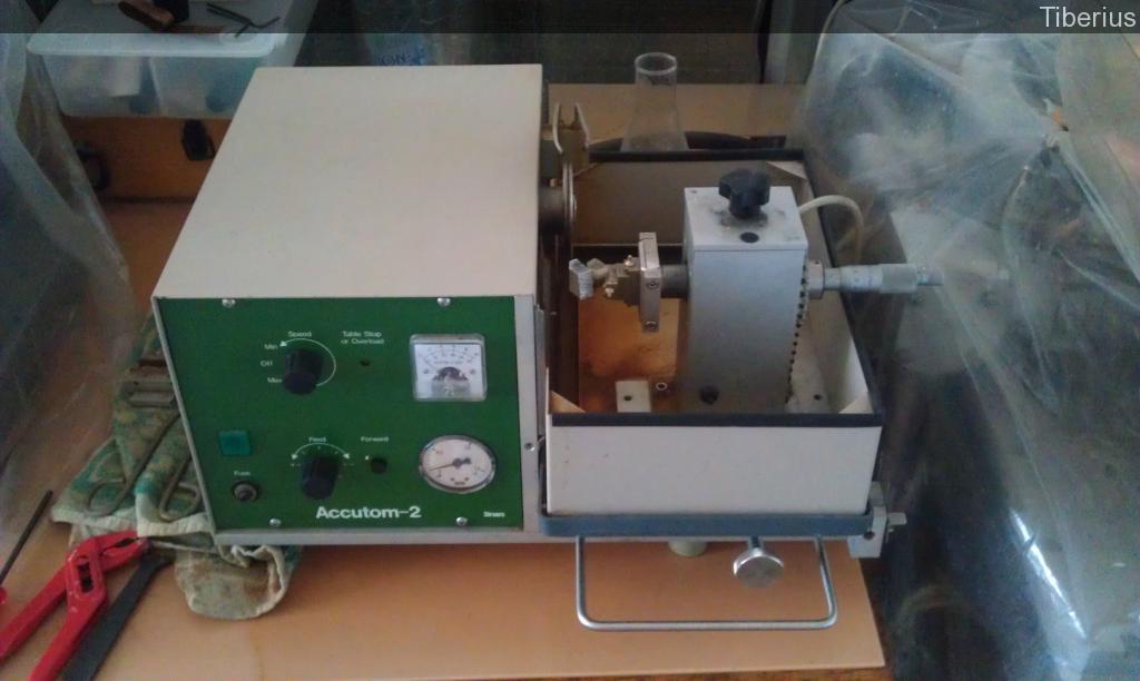
Our old but good Accutom-2. In the corporation of good, even a normal photo of this device was not found.
Probably, he acted foolishly that he did not take a video of the process of cutting the chip itself, but what to do - c'est la vie. When I had 3 pieces in my hands, there was no limit to disappointment. It turned out that the cut was rather coarse (although I expected that the microtome could cut exactly and leave a smooth surface after itself), and I had to grind and polish the end surface of the chip for a long time and hard, which I then examined under an electron microscope.
')
About the benefits of polishing
By the way, the benefits of polishing are visible to the naked eye, more precisely armed, but only with an optical microscope:
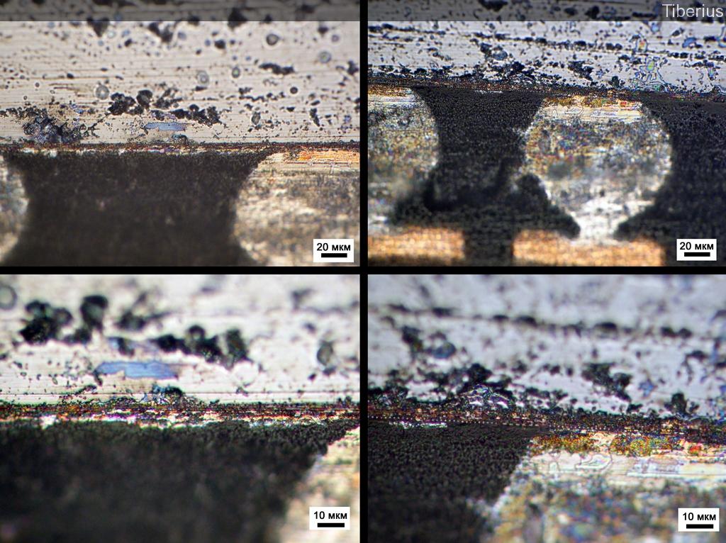
Left photos before polishing, right - after. The top row of photos is an increase of 50x, the bottom one is 100x.
After polishing (photos on the right), copper contacts connecting individual chip structures are already visible at 50x magnification. Before polishing, they, of course, also look through the dust and chippings formed after cutting, but it is unlikely to make out the individual contacts.
Electron microscopy
Optics give a 100-200 magnification magnification, but this cannot be compared with 100,000 or even 1,000,000 magnification, which an electron microscope can produce (theoretically, for TEM, the resolution is tenths or even hundredths of an angstrom, but due to some realities life such a resolution is not achieved). In addition, the chip is made according to the 90 nm process technology, and it is quite problematic to see separate elements of the integrated circuit using optics. But electrons, coupled with certain types of detection ( SE2 - secondary electrons) allow us to visualize the difference in the chemical composition of the material and, thus, look into the very silicon heart of our patient, namely, to see the sink / source, but more on that below.
Printed circuit board
So let's get started. The first thing we see is a printed circuit board on which the silicon crystal itself is mounted. It is attached to the laptop motherboard using BGA soldering. During the development of the lecture for schoolchildren, I used quite detailed publications from Intel on Habré, but recently I found a couple of video fragments from the Discovery channel about silicon electronics. For example, in this video snapshot it is described how the silicon chip is mounted on the substrate, as well as how these small (~ 0.5 mm in diameter) tin balls are arranged in an orderly manner on the printed circuit board. The Chinese with their diligence and zeal have absolutely nothing to do with it:

BGA soldering.
BGA soldering.
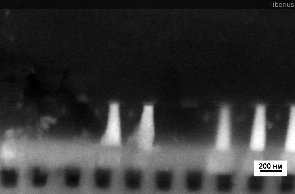
The crystal itself is installed on a kind of BGA, let's call it “mini” -BGA. These are the same tin balls that connect a small piece of silicon with a large multi-layer printed circuit board, only their size is much smaller.
Comparison of BGA and mini-BGA soldering.
Comparison of BGA and mini-BGA soldering.
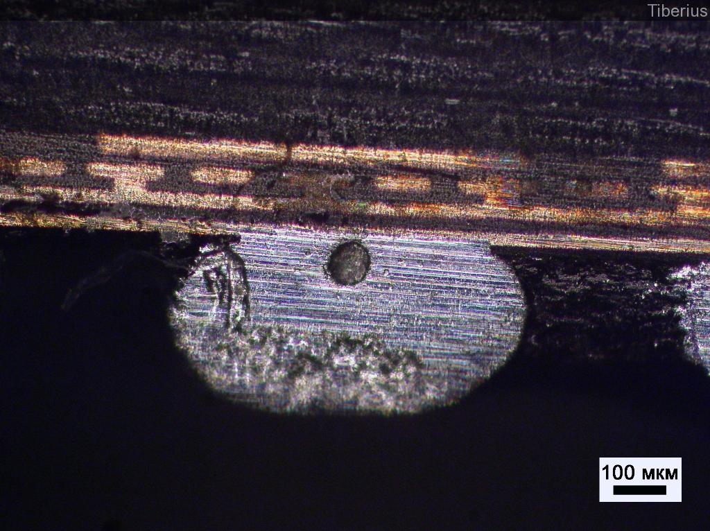
By the way, there are a lot of “balls” between the crystal and the printed circuit board, which, apparently, are a kind of filler of the empty space between these elements and, possibly, contribute to heat removal from the chip itself to the PCB.
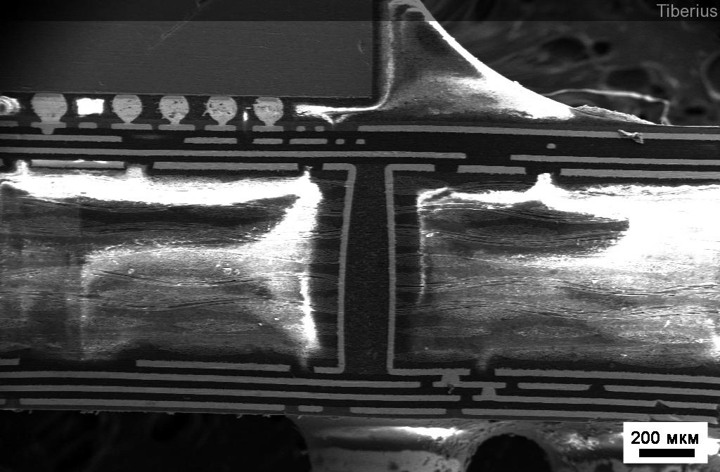
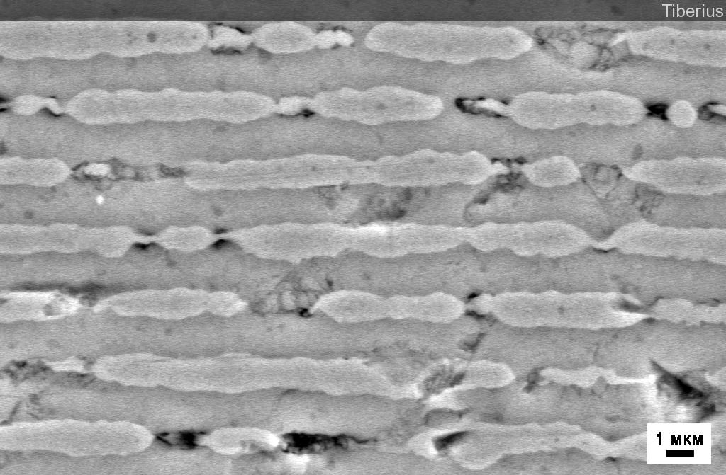
Many spherical particles fill the space between the chip and the printed circuit board. And you see already looking contacts on the video chip itself ?!
Next will be a few photos of the PCB. It turned out to be 8 layers, with all the layers somehow connected to each other. And yet - the board material is “wavy”; this is noticeable both in optical photographs and in images obtained with an electron microscope. Who knows why?
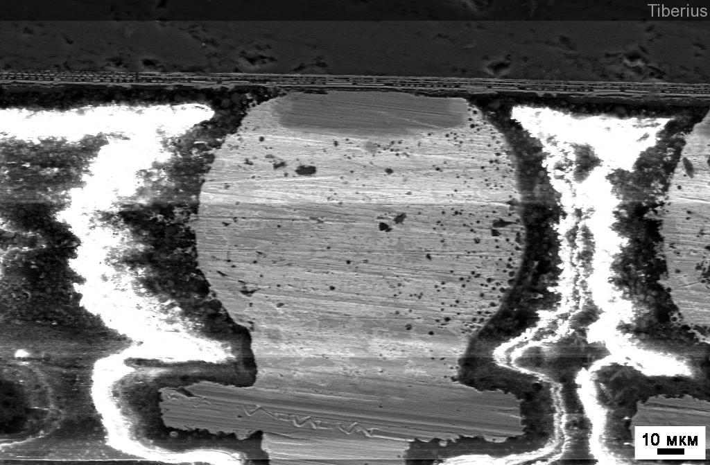
Strapping element
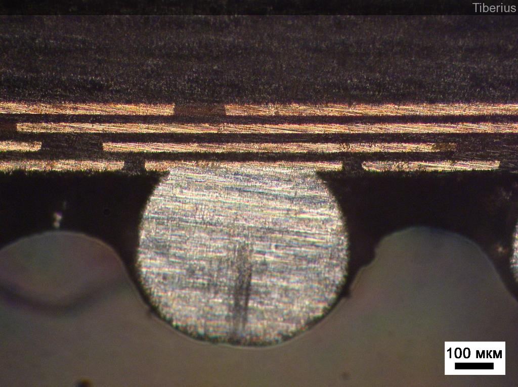
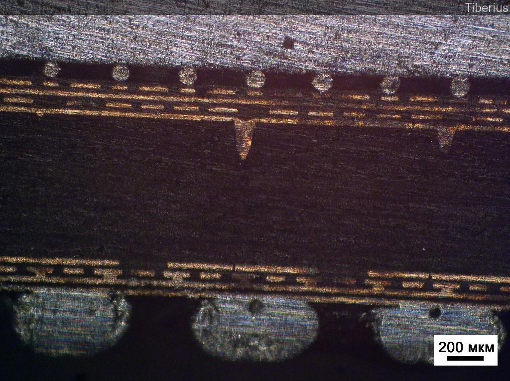
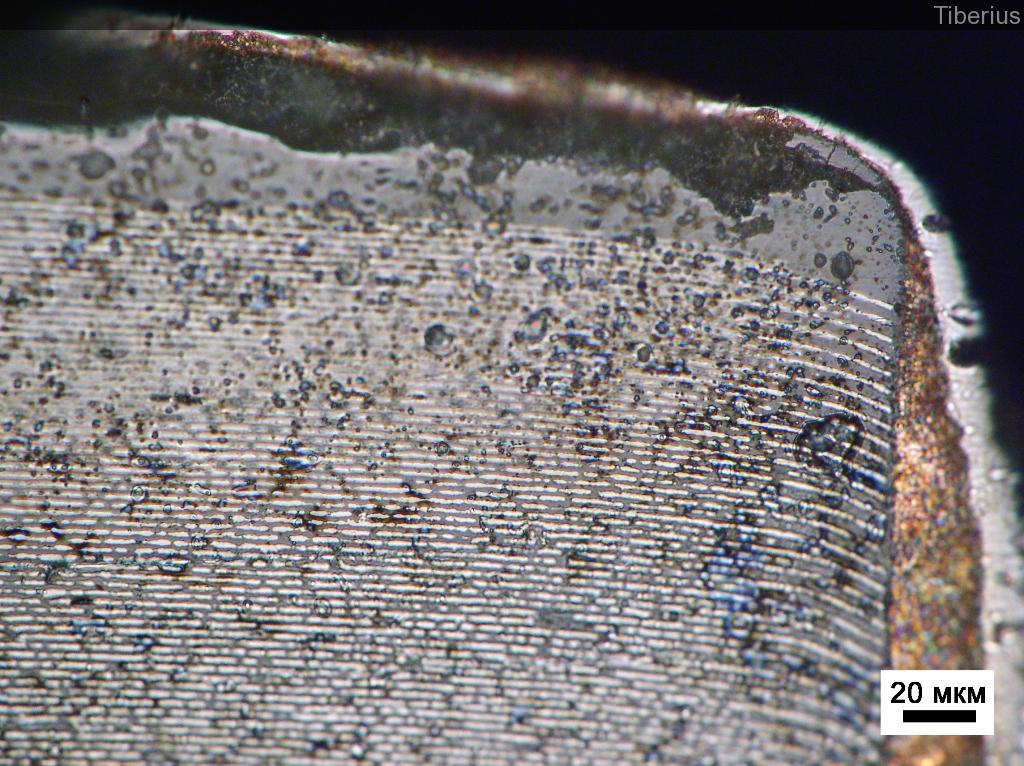
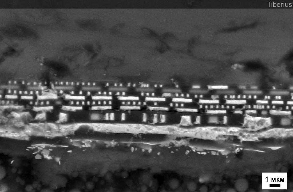
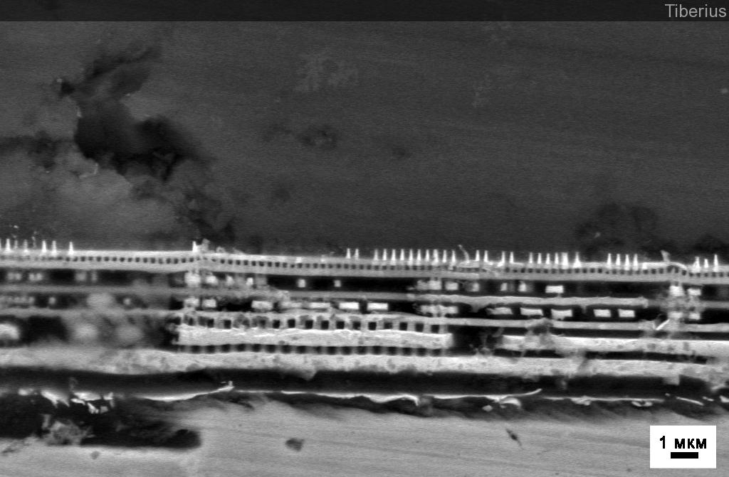
Microtome allowed to carefully cut one of the elements of the strapping, which, apparently, is either an SMD resistor or a capacitor. But, to be honest, I expected to see anything, just not a striped structure (i.e. this element is assembled in layers of several materials, as evidenced by the difference in contrast), so if you have knowledgeable people, your comments will help you to understand.
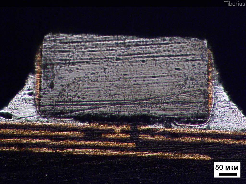
Optical photograph of the video chip trimmer.

Optical photograph of the video chip trimmer.
Optical photograph of the video chip trimmer.
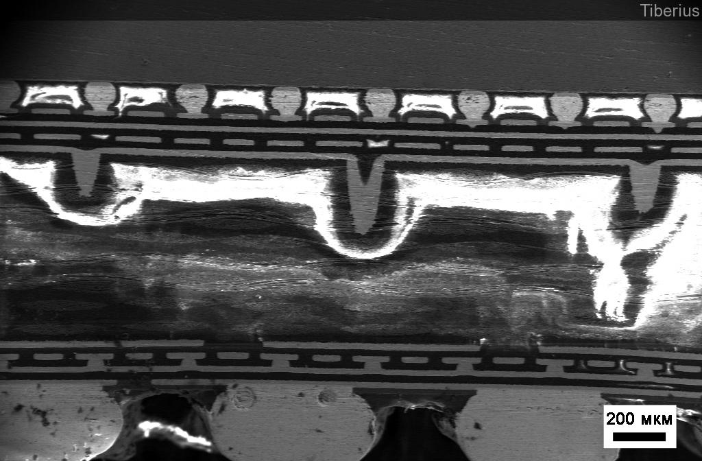
SAM photo of the video chip strapping element.
SAM photo of the video chip strapping element.
Crystal NVidia 8600GT in person
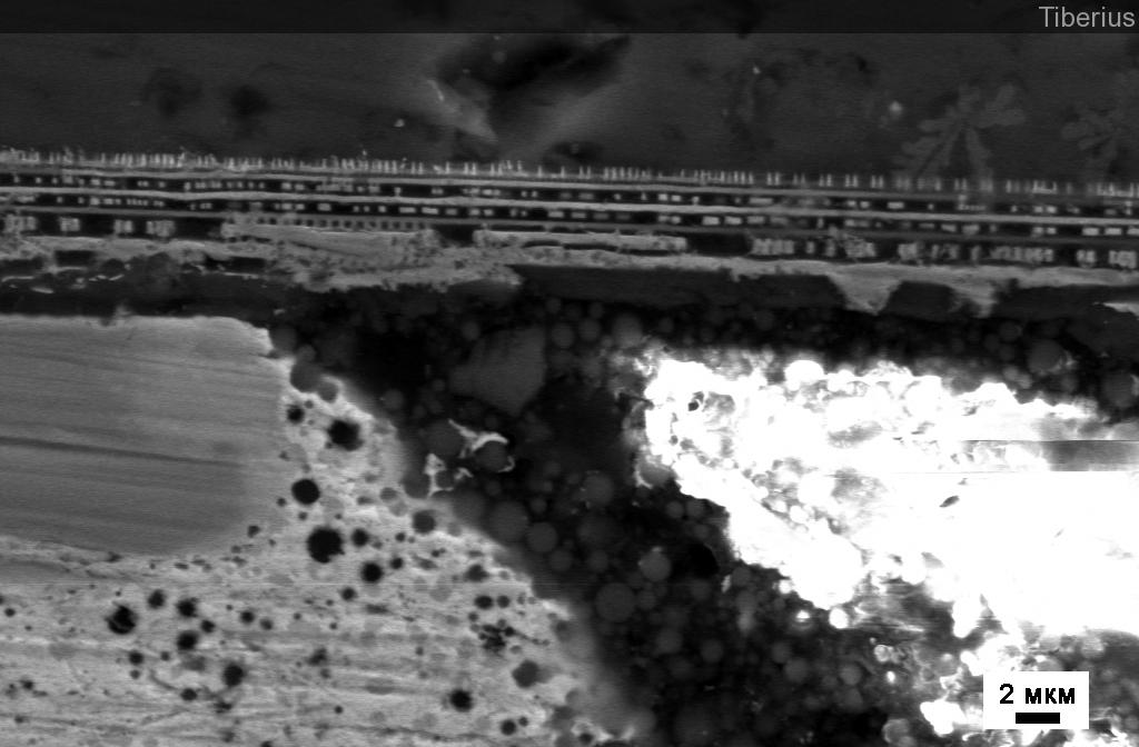
So, it seems we saw all the elements of the NVidia 8600 GT chip, except for the most important thing - the device of the stone itself, or rather a very thin layer on it. You can learn about how quartz sand turns into high-purity monocrystalline silicon from an Intel blog or from the following video, again from the Discovery channel:
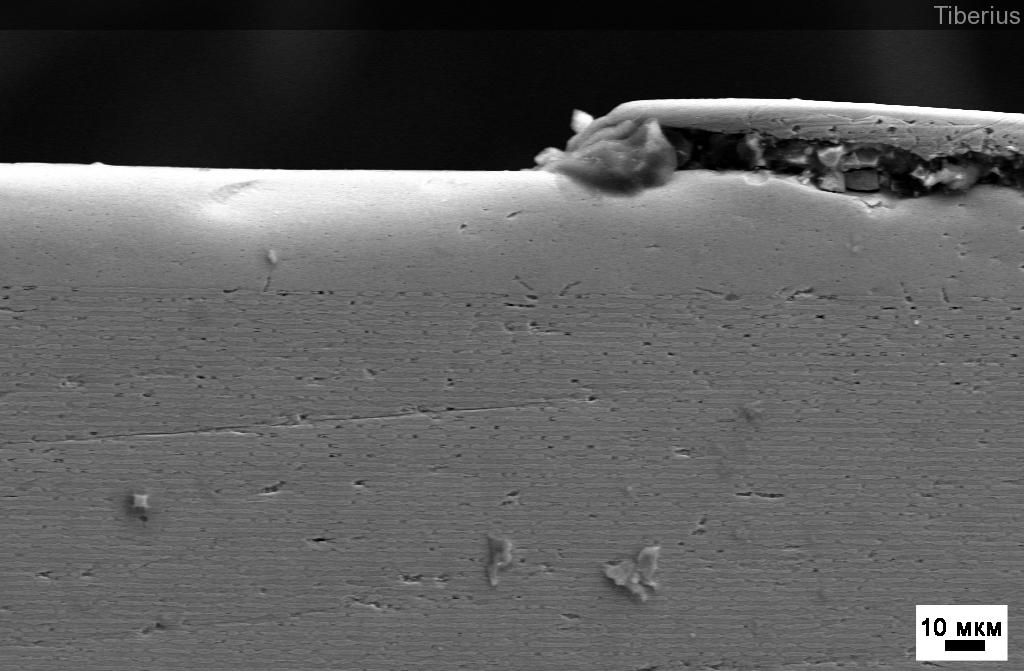
In order to drive electrons through their copper and semiconductor contacts, silicon plates went through many processing steps, and I took it and spoiled everything, prepared the poor chip. But I will not torment for a long time ... That's why I suffered for so long, and what I wanted to see - the individual elements, made according to the 90 nm process technology:
Separate elements of modern computer equipment.
The barely noticeable difference in contrast - these are the very drains / sources that help us to work with you at the computer, play computer games, watch movies, listen to music, etc. The size of the structures, according to my calculations, is about 114 nm, taking into account ~ 10% in the scale and calculations, as well as the features of lithography, this figure is in very good agreement with the stated technical process.
Next will be some more photos of the video chip:


Conclusion
A lot of what I saw inside the video chip struck me. The strapping element is generally a striped masterpiece. And I was happy to share this with the students at the opening of the Nanotechnology Olympiad, the in-person tour of which was held in Moscow in April. At the opening I had a chance to read the prepared lecture.
Of course, publications from Intel, photos found on the Internet with the help of the corporation of good, beautiful pictures and animations are a great thing, allowing you to quickly obtain the required information and knowledge. However, when you personally cut the chip, study it, not looking up from the monitor screen for hours, and you see that the technical process is really 90 nm, that someone could create, calculate this whole structure down to the smallest details, then at that moment you feel joy and pride in humanity that has created such a perfect product. It's just wow !
PS If this material is of interest to the respected habra people, then you can continue. Already in semi-finished form, a dead and prepared flash drive, HDD, a piece of a CD disk and a resistive display of a chinaphone lie neatly in the box today.
PPS While I was cutting out the time to prepare the material on Habré a similar article appeared on the Pentium III , so we will consider this a continuation.
First , the full list of published articles on Habré:
Opening the Nvidia 8600M GT chip , a more detailed article is given here: Modern chips - a view from the inside
An inside look: CD and HDD
An inside look: LED bulbs
An inside look: the LED industry in Russia
An inside look: Flash and RAM
An inside view: the world around us
An inside look: LCD and E-Ink displays
An inside look: matrix digital cameras
An inside look: Plastic Logic
An inside look: RFID and other tags
An inside look: graduate school at EPFL. Part 1
An inside look: graduate school at EPFL. Part 2
An inside view: the world around us - 2
An inside view: the world around us - 3
An inside look: the world around us - 4
An inside look: 13 LED lamps and a bottle of rum. Part 1
An inside look: 13 LED lamps and a bottle of rum. Part 2
An inside look: 13 LED lamps and a bottle of rum. Part 3
An inside look: IKEA LED strikes back
An inside view: are Fillament lamps good for you?
and 3DNews:
Microview: a comparison of modern smartphones displays
Secondly , in addition to the blog on HabraHabr , articles and videos can be read and viewed on Nanometer.ru , YouTube , and Dirty .
Thirdly , if you, dear reader, liked the article or you want to stimulate writing new ones, then act according to the following maxim: “pay what you want”
Yandex.Money 41001234893231
WebMoney (R296920395341 or Z333281944680)
Sometimes briefly, and sometimes not so much about the news of science and technology, you can read on my Telegram channel - welcome;)
Source: https://habr.com/ru/post/127786/
All Articles