Autopsy Pentium III, photographs under the microscope
Everyone was holding an ordinary microprocessor in their hands, but it hardly occurred to anyone to cut it and examine it under a scanning electron microscope. This is exactly what the Swedish teacher Kristian Storm did to demonstrate the microchip device to students. Photos are stunning: the quality allows you to see the individual layers of the processor. Apparently, about this procedure was used by Soviet engineers, who analyzed and copied Western designs. Approximately the same thing is being done now to study the products of competitors.
All photos are clickable and available in high resolution.
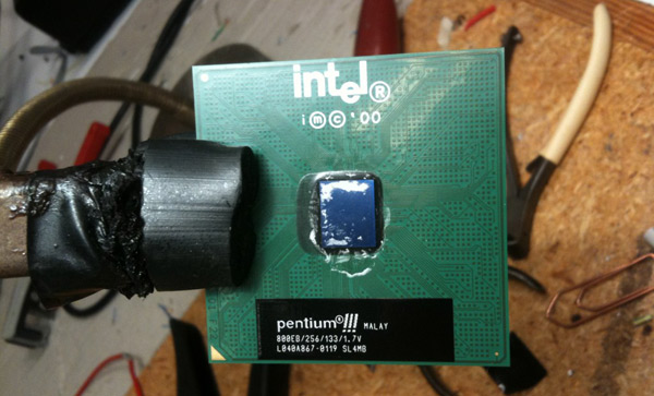
Christian Storm used a P-III processor. To begin with, it was necessary to remove the microchip directly from the plastic case (blue), which is located in the center of the circuit board (green).
')
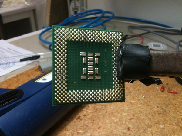
As can be seen on the back of the circuit board, it is needed to output the contacts from the microprocessor - from each contact on the processor a signal goes to a separate pin on the board.
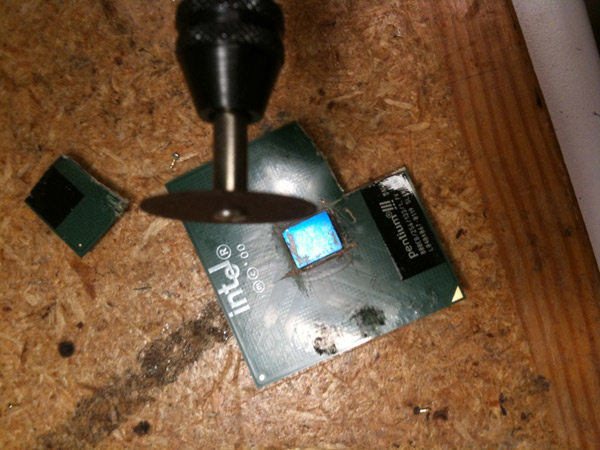
At first, Christian thought that he would be able to separate the microprocessor by heating, but did not achieve anything but a nasty smell. Then I had to use brute force and cut the corresponding section. With the help of forceps and a scalpel, he pulled out the same chip, slightly damaging it in the process (however, Christian was already going to break the processor for the shooting).
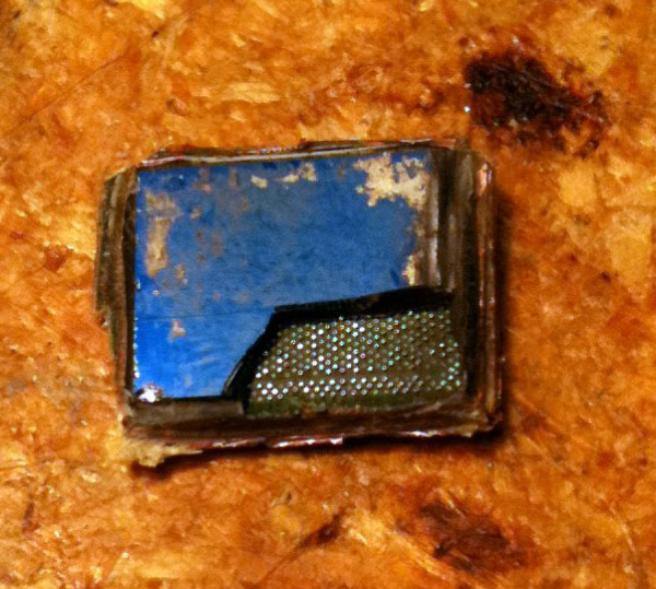
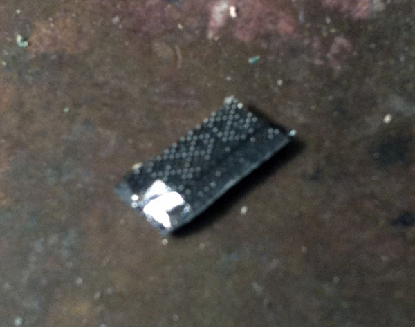
That's what happened as a result. On the reverse side of the chip under the broken blue case visible contacts on the chip. Previously, they were connected to pins on the board.
Here the chip is cleared of plastic.
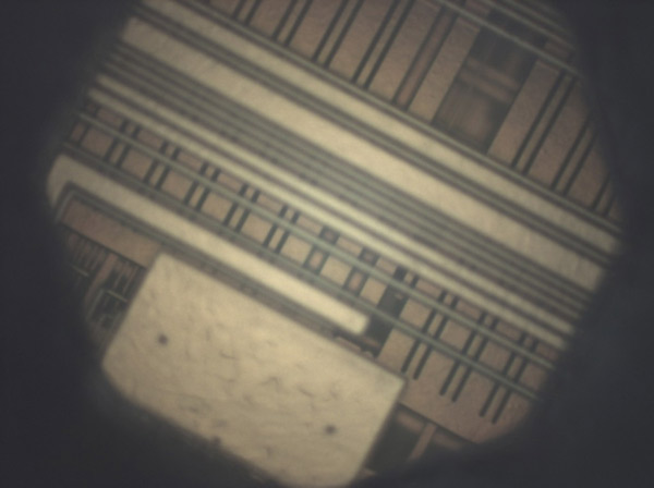
Now the fun begins: a microscope enters the work. First, the usual optical. Under the microscope, we look at a fragment of a microprocessor with the same contacts.
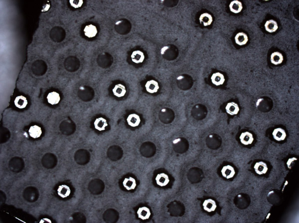
If you look closer, you can distinguish the structure inside the holes for the contacts.
The processor consists of a set of metal layers on top of each other, they are clearly visible through the holes for the contacts.
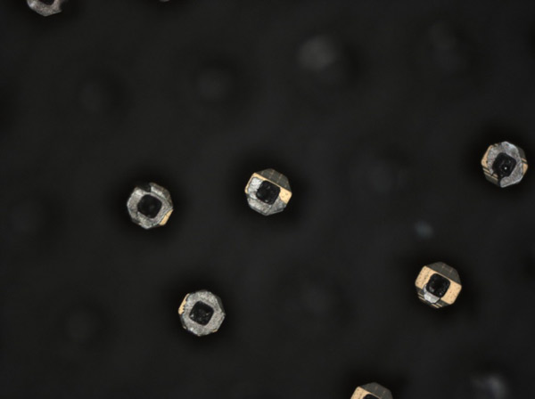
By changing the focus on the microscope, you can examine these layers in turn. Here is the top layer.

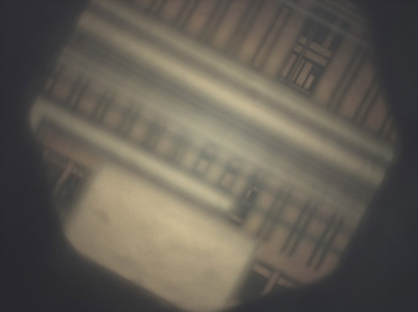
Middle layer
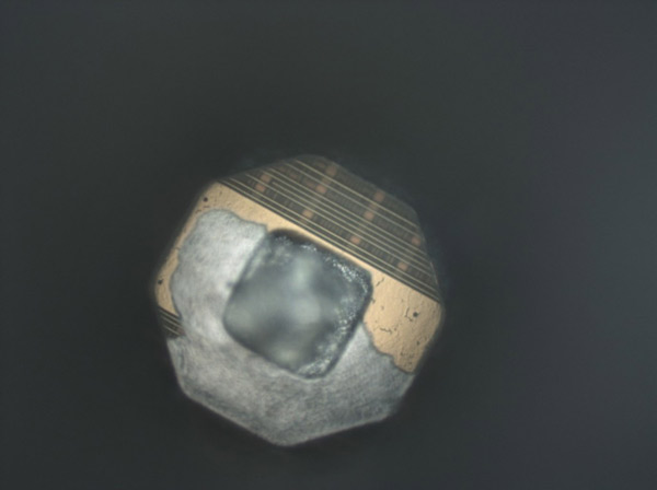
And the bottom layer.
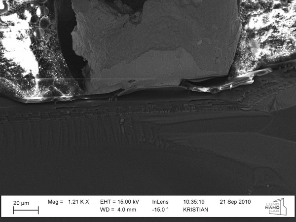
Since the optical microscope does not provide the necessary detail, Christian decided to use a scanning electron microscope. To see the inside of the processor, he broke it apart and began to look at the scrapping sites. Below you can see a series of consecutive photos with gradually increasing resolution.
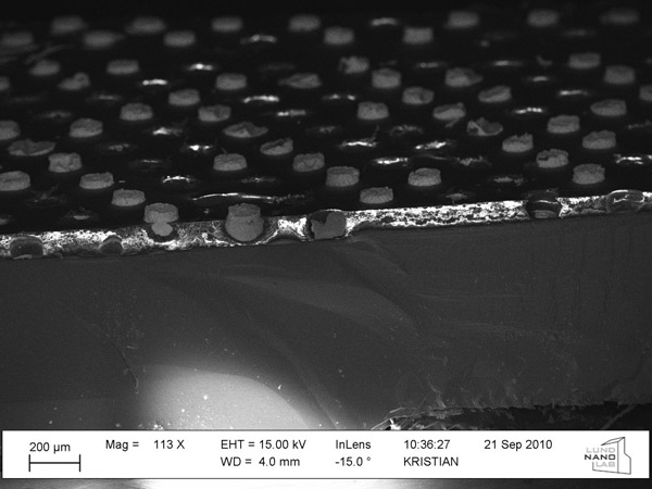
The microcircuit is turned upside down, so that at the top is a row of contacts that were previously attached to the circuit board. At first, nothing special can be seen. The light material between the contacts is apparently some kind of polymer to fill the space.
But then the outlines of a structure begin to appear.

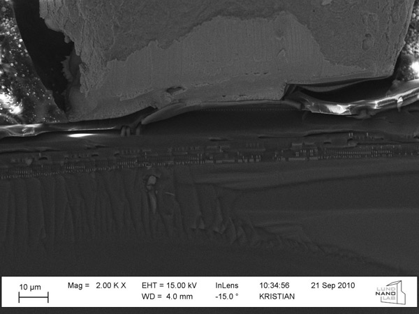
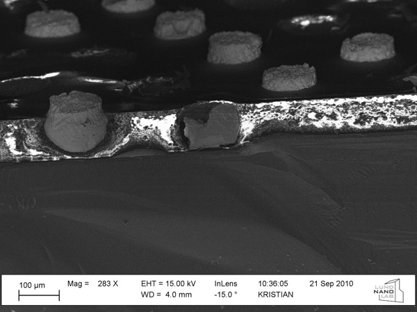
With further magnification, the layers are already clearly visible. You can even count their number: six.

The thickness of the lower metal layer is about 200-250 nm. The P-III processor was manufactured using a 250 nm process technology, and later - 180 nm, so this lower layer is the last layer with transistors, a further approximation will not show new elements.
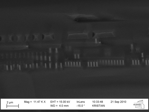
Here's what the picture looks like in an improved form.
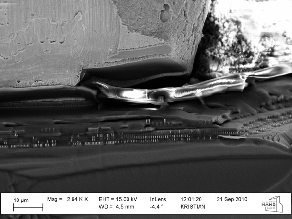
The last photo was taken on the same scale, just above. In one place, the body accidentally broke off, so that the internal structure was exposed.
There are several metal layers in each other, but Christian could not take layer-by-layer photos and get directly to the transistors (bottom layer), because he does not know how to carefully remove the layers from the chip.
All photos are clickable and available in high resolution.
Christian Storm used a P-III processor. To begin with, it was necessary to remove the microchip directly from the plastic case (blue), which is located in the center of the circuit board (green).
')
As can be seen on the back of the circuit board, it is needed to output the contacts from the microprocessor - from each contact on the processor a signal goes to a separate pin on the board.
At first, Christian thought that he would be able to separate the microprocessor by heating, but did not achieve anything but a nasty smell. Then I had to use brute force and cut the corresponding section. With the help of forceps and a scalpel, he pulled out the same chip, slightly damaging it in the process (however, Christian was already going to break the processor for the shooting).
That's what happened as a result. On the reverse side of the chip under the broken blue case visible contacts on the chip. Previously, they were connected to pins on the board.
Here the chip is cleared of plastic.
Now the fun begins: a microscope enters the work. First, the usual optical. Under the microscope, we look at a fragment of a microprocessor with the same contacts.
If you look closer, you can distinguish the structure inside the holes for the contacts.
The processor consists of a set of metal layers on top of each other, they are clearly visible through the holes for the contacts.
By changing the focus on the microscope, you can examine these layers in turn. Here is the top layer.
Middle layer
And the bottom layer.
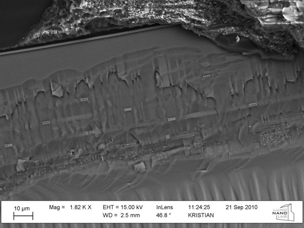
Since the optical microscope does not provide the necessary detail, Christian decided to use a scanning electron microscope. To see the inside of the processor, he broke it apart and began to look at the scrapping sites. Below you can see a series of consecutive photos with gradually increasing resolution.
The microcircuit is turned upside down, so that at the top is a row of contacts that were previously attached to the circuit board. At first, nothing special can be seen. The light material between the contacts is apparently some kind of polymer to fill the space.
But then the outlines of a structure begin to appear.
With further magnification, the layers are already clearly visible. You can even count their number: six.
The thickness of the lower metal layer is about 200-250 nm. The P-III processor was manufactured using a 250 nm process technology, and later - 180 nm, so this lower layer is the last layer with transistors, a further approximation will not show new elements.
Here's what the picture looks like in an improved form.
The last photo was taken on the same scale, just above. In one place, the body accidentally broke off, so that the internal structure was exposed.
There are several metal layers in each other, but Christian could not take layer-by-layer photos and get directly to the transistors (bottom layer), because he does not know how to carefully remove the layers from the chip.
Source: https://habr.com/ru/post/127205/
All Articles