VHDL delay element
When designing various digital devices, in particular, controllers, it is required to organize a delay in the supply of the same signal to different outputs of the FPGA or to other elements inside the FPGA.
To begin, consider a similar situation with discrete logic. Usually, if a developer has a microcircuit with six NOT gates (for example, 1551), he uses a series connection of two elements as a delay element (value 10 ... 20 nanoseconds). Sometimes between them he inserts an RC circuit, with which you can make a delay time from 10 to 150 ns.
In the FPGA chip, the delay in this way can NOT be organized. It's all about features of the synthesis of the project. The synthesis program perceives double negation as an extra link (as an error) and eliminates it. On RC - circuits it is also impossible to organize a delay, because the FPGA does not tolerate capacitive load badly. Therefore, to organize the delay, I recommend the following method. Sketched it looks like this:
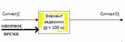
The Ct signal is the same C signal, only delayed by 100 ns.
')
The reference time signal is a pulse signal with a specific frequency that we need to use in the delay element. The period of this signal is the minimum possible time for which we can delay the t signal relative to C. In our case, the reference time signal period is 50 ns (frequency is 20 MHz).
Now I present to your attention the "iron" structure of the delay element:
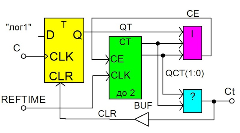
In this structure, there is only one incomprehensible element of blue “?”. In fact, it is just a product of combinatorial logic. I will not decipher the structure of this element, I will give only its truth table:

The element T is an ordinary D-trigger with synchronization on the signal's front C. The element CT is the counter of pulses of the reference frequency (time) REFTIME. In addition to the CLK clock input, it has a CE enable input. To form a delay time of 100 ns, the counter must complete the counting counting to two (50 x 2 = 100). This parameter must be subsequently specified in the counter VHDL code. Element pink - 3-OR. A BUF buffer is required to separate the output signal Ct and the internal signal CLR.
An experienced developer does not need to explain how this scheme works, but since this article is also read by novice developers, I’ll give a brief description of how the scheme works.
External signal REFTIME with a frequency of 20 MHz is fed to the counter CT constantly. The “D” input of trigger T is permanently tied to a logical one. When applying to the CLK input of the signal edge trigger C, the first unit appears at the input of the 3-OR element. This element immediately allows the counter to be counted. As soon as the counter counts to 2x, the D-flip-flop is immediately reset to the state of logical zero, and along with the next REFTIME pulse, logical zeroes appear at its outputs. At the same time, an account is prohibited.
The peculiarity of this scheme is that the signal C is not only delayed by 100 ns, but to the heap its duration is also shortened to 50 ns (that is, before the period of the reference signal). In most cases, this feature is not critical and you just can not pay attention. But this feature can be used and purposefully for the formation of the pulse duration.
I present to you the text of the VHDL program of the delay element:
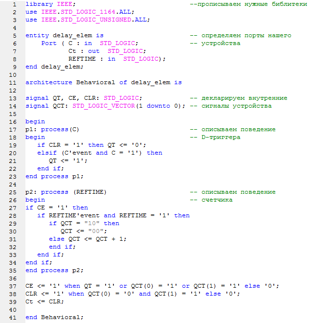
The process labeled p1 describes the behavior of the D-trigger, while the process labeled p2 is the counter.
To begin, consider a similar situation with discrete logic. Usually, if a developer has a microcircuit with six NOT gates (for example, 1551), he uses a series connection of two elements as a delay element (value 10 ... 20 nanoseconds). Sometimes between them he inserts an RC circuit, with which you can make a delay time from 10 to 150 ns.
In the FPGA chip, the delay in this way can NOT be organized. It's all about features of the synthesis of the project. The synthesis program perceives double negation as an extra link (as an error) and eliminates it. On RC - circuits it is also impossible to organize a delay, because the FPGA does not tolerate capacitive load badly. Therefore, to organize the delay, I recommend the following method. Sketched it looks like this:
The Ct signal is the same C signal, only delayed by 100 ns.
')
The reference time signal is a pulse signal with a specific frequency that we need to use in the delay element. The period of this signal is the minimum possible time for which we can delay the t signal relative to C. In our case, the reference time signal period is 50 ns (frequency is 20 MHz).
Now I present to your attention the "iron" structure of the delay element:
In this structure, there is only one incomprehensible element of blue “?”. In fact, it is just a product of combinatorial logic. I will not decipher the structure of this element, I will give only its truth table:
The element T is an ordinary D-trigger with synchronization on the signal's front C. The element CT is the counter of pulses of the reference frequency (time) REFTIME. In addition to the CLK clock input, it has a CE enable input. To form a delay time of 100 ns, the counter must complete the counting counting to two (50 x 2 = 100). This parameter must be subsequently specified in the counter VHDL code. Element pink - 3-OR. A BUF buffer is required to separate the output signal Ct and the internal signal CLR.
An experienced developer does not need to explain how this scheme works, but since this article is also read by novice developers, I’ll give a brief description of how the scheme works.
External signal REFTIME with a frequency of 20 MHz is fed to the counter CT constantly. The “D” input of trigger T is permanently tied to a logical one. When applying to the CLK input of the signal edge trigger C, the first unit appears at the input of the 3-OR element. This element immediately allows the counter to be counted. As soon as the counter counts to 2x, the D-flip-flop is immediately reset to the state of logical zero, and along with the next REFTIME pulse, logical zeroes appear at its outputs. At the same time, an account is prohibited.
The peculiarity of this scheme is that the signal C is not only delayed by 100 ns, but to the heap its duration is also shortened to 50 ns (that is, before the period of the reference signal). In most cases, this feature is not critical and you just can not pay attention. But this feature can be used and purposefully for the formation of the pulse duration.
I present to you the text of the VHDL program of the delay element:
The process labeled p1 describes the behavior of the D-trigger, while the process labeled p2 is the counter.
Source: https://habr.com/ru/post/126431/
All Articles