Analog to digital conversion for beginners
This article discusses the main issues related to the principle of operation of various types of ADCs. At the same time, some important theoretical calculations concerning the mathematical description of the analog-to-digital conversion remained outside the scope of the article, but there are references that interested readers can find a more in-depth look at the theoretical aspects of the ADC. Thus, the article deals with a greater degree of understanding of the general principles of functioning of the ADC, than a theoretical analysis of their work.
 "
"
Introduction
')
As a starting point we give the definition of analog-to-digital conversion. Analog-to-digital conversion is the process of converting an input physical quantity into its numerical representation. An analog-to-digital converter is a device that performs this conversion. Formally, the input value of an ADC can be any physical quantity — voltage, current, resistance, capacitance, pulse repetition rate, shaft angle of rotation, etc. However, for definiteness, in the future, under ADC, we will understand only voltage-code converters.
The concept of analog-digital conversion is closely related to the concept of measurement. Under the measurement refers to the process of comparing the measured value with a certain standard, when analog-to-digital conversion is the comparison of the input value with a certain reference value (as a rule, with the reference voltage). Thus, analog-to-digital conversion can be considered as a measurement of the input signal value, and all metrology concepts, such as measurement errors, are applicable to it.
The main characteristics of the ADC
The ADC has many characteristics, of which the main ones are the conversion frequency and bit depth. The frequency of conversion is usually expressed in samples per second (samples per second, SPS), bit depth - in bits. Modern ADCs can be up to 24-bit wide and can be converted to GSPS units (of course, not simultaneously). The higher the speed and bitness, the harder it is to obtain the required characteristics, the more expensive and more complex the converter. The conversion speed and bit depth are related to each other in a certain way, and we can increase the effective conversion digit capacity by sacrificing speed.
Types of ADC
There are many types of ADCs, but in this article we will limit ourselves to considering only the following types:
There are also other types of ADCs, including conveyor and combined types, consisting of several ADCs with (in general) different architectures. However, the above ADC architectures are most indicative of the fact that each architecture occupies a certain niche in the general range of speed-digit capacity.
ADC direct (parallel) conversion has the highest speed and the lowest bit depth. For example, Texas Instruments' TLC5540 parallel conversion ADC has a speed of 40MSPS with a bit capacity of only 8 bits. This type of ADC can have a conversion rate of up to 1 GSPS. It can be noted here that pipelined ADCs have even greater speed, however they are a combination of several ADCs with lower speed and their consideration is beyond the scope of this article.
The average niche in the range of digit-speed occupy the ADC successive approximation. Typical values are 12–18 bits at a conversion frequency of 100KSPS-1MSPS.
The highest accuracy is achieved by a sigma-delta A / D converter, having a bit width up to and including 24 bits and speed from SPS units to KSPS units.
Another type of ADC that has found application in the recent past is an integrating ADC. Integrating ADCs are now almost completely superseded by other types of ADCs, but can be found in older measuring devices.
ADC direct conversion
Direct conversion ADCs were widely used in the years 1960-1970, and were made in the form of integrated circuits in the 1980s. They are often used as part of "pipelined" ADCs (not considered in this article), and have a bit depth of 6-8 bits at speeds up to 1 GSPS.
The architecture of the direct conversion ADC is depicted in Fig. one

Fig. 1. Block diagram of the ADC direct conversion
The principle of operation of the ADC is extremely simple: the input signal is fed simultaneously to all the “plus” inputs of the comparators, and to the “minus” inputs are supplied a series of voltages obtained from the reference by dividing by resistors R. For the circuit in fig. 1 this row will be like this: (1/16, 3/16, 5/16, 7/16, 9/16, 11/16, 13/16) Uref, where Uref is the reference voltage of the ADC.
Let a voltage equal to 1/2 Uref be applied to the ADC input. Then the first 4 comparators will work (if we count from below), and logical units will appear at their outputs. The priority encoder will generate a binary code from the “column” of the units, which is fixed by the output register.
Now become clear advantages and disadvantages of such a converter. All comparators work in parallel, the delay time of the circuit is equal to the delay time in one comparator plus the delay time in the encoder. The comparator and the encoder can be made very fast, as a result, the whole circuit has a very high speed.
But to get N digits, you need 2 ^ N comparators (and the complexity of the encoder also grows as 2 ^ N). The diagram in fig. 1. contains 8 comparators and has 3 bits, to get 8 bits, 256 comparators are needed, for 10 bits - 1024 comparators, for a 24-bit ADC they would need more than 16 million. However, the equipment has not yet reached such heights.
ADC sequential approximation
The ADC sequential approximation implements the "weighting" algorithm, which goes back to Fibonacci. In his book Liber Abaci (1202), Fibonacci considered the “problem of choosing the best weights system”, that is, finding such a number of weights weights that would require to find the weight of the object the minimum number of weighings on the lever weights. The solution to this problem is a “binary” set of weights. More information about the Fibonacci problem can be found, for example, here: http://www.goldenmuseum.com/2015AMT_rus.html .
A successive approximation analog-to-digital converter (SAR, Successive Approximation Register) measures the magnitude of the input signal by performing a series of “weightings,” that is, comparing the magnitude of the input voltage with a number of values generated as follows:
1. at the first step, the output of the built-in digital-to-analog converter is set to 1 / 2Uref (hereinafter we assume that the signal is in the interval (0 - Uref).
2. if the signal is greater than this value, then it is compared with the voltage lying in the middle of the remaining interval, that is, in this case, 3 / 4Uref. If the signal is less than the set level, the next comparison will be made with a smaller half of the remaining interval (ie, with a level of 1 / 4Uref).
3. Step 2 is repeated N times. Thus, N comparisons (“weightings”) produce N bits of the result.
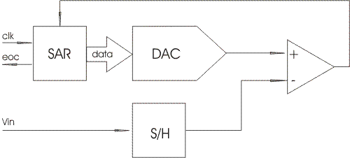
Fig. 2. Block diagram of the ADC sequential approximation.
Thus, the ADC sequential approximation consists of the following nodes:
1. The comparator. It compares the input value and the current value of the "weight" voltage (in Fig. 2. indicated by a triangle).
2. Digital-to-analog converter (Digital to Analog Converter, DAC). It generates a “weight” voltage value based on the input digital code.
3. Register successive approximation (Successive Approximation Register, SAR). It implements a sequential approximation algorithm, generating the current code value applied to the input of the DAC. By its name is named all the architecture of the ADC.
4. Sampling-storage scheme (Sample / Hold, S / H). For the operation of this ADC, it is of fundamental importance that the input voltage maintains a constant value throughout the entire conversion cycle. However, “real” signals tend to change over time. The sampling-storage scheme “remembers” the current value of the analog signal, and keeps it unchanged throughout the entire operation cycle of the device.
The advantage of the device is a relatively high conversion speed: the conversion time of the N-bit ADC is N clock cycles. The accuracy of the conversion is limited by the accuracy of the internal DAC and can be 16-18 bits (24-bit SAR ADCs, for example, AD7766 and AD7767, are now appearing).
Delta-Sigma ADC
And finally, the most interesting type of ADC is the sigma-delta ADC, sometimes referred to as charge-balancing ADC in literature. The structure of the sigma-delta ADC is shown in Fig. 3

Fig.3. Block diagram of sigma-delta ADC.
The principle of operation of this ADC is somewhat more complicated than that of other types of ADCs. Its essence is that the input voltage is compared with the voltage value accumulated by the integrator. Pulses of positive or negative polarity are applied to the integrator input, depending on the result of the comparison. Thus, this ADC is a simple tracking system: the voltage at the integrator output "monitors" the input voltage (Fig. 4). The result of this scheme is a stream of zeros and ones at the output of the comparator, which is then passed through a digital low-pass filter, resulting in an N-bit result. LPF in fig. 3. Combined with a “decimator”, a device that reduces the frequency of following samples by “thinning”.

Fig. 4. Sigma-delta ADC as a tracking system
For the sake of rigor, it must be said that in fig. 3 shows a block diagram of a sigma-delta first-order ADC. A second-order sigma-delta ADC has two integrators and two feedback loops, but will not be considered here. Those interested in this topic may refer to [3].
In fig. 5 shows the signals in the ADC at the zero level at the input (top) and at the level Vref / 2 (bottom).

Fig. 5. Signals in the ADC at different signal levels at the input.
More clearly the work of the sigma-delta ADC is demonstrated by a small program located here: http://designtools.analog.com/dt/sdtutorial/sdtutorial.html.
Now, without going into complex mathematical analysis, let us try to understand why sigma-delta ADCs have a very low level of intrinsic noise.
Consider the block diagram of a sigma-delta modulator, shown in Fig. 3, and present it in this form (Fig. 6):
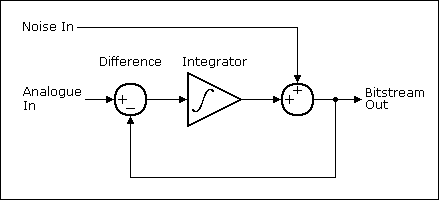
Fig. 6. Block diagram of sigma-delta modulator
Here the comparator is represented as an adder, which summarizes the continuous wanted signal and quantization noise.
Let the integrator have a transfer function of 1 / s. Then, by representing the useful signal as X (s), the output of the sigma-delta modulator as Y (s), and the quantization noise as E (s), we obtain the transfer function of the ADC:
Y (s) = X (s) / (s + 1) + E (s) s / (s + 1)
That is, in fact, the sigma-delta modulator is a low-pass filter (1 / (s + 1)) for the wanted signal, and a high-pass filter (s / (s + 1)) for noise, and both filters have the same cut-off frequency. Noise, concentrated in the high-frequency region of the spectrum, is easily removed by a digital low-pass filter that stands after the modulator.
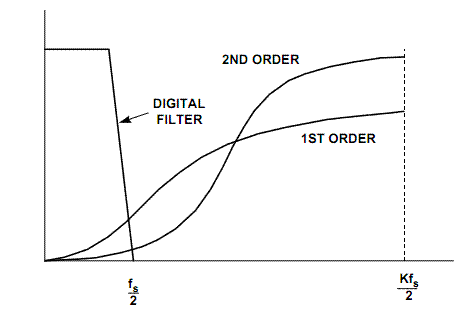
Fig. 7. The phenomenon of "crowding out" of noise in the high-frequency part of the spectrum
However, it should be understood that this is an extremely simplified explanation of the phenomenon of noise shaping in a sigma-delta ADC.
So, the main advantage of the sigma-delta ADC is high accuracy, due to the extremely low level of intrinsic noise. However, to achieve high accuracy, it is necessary that the cutoff frequency of the digital filter is as low as possible, many times smaller than the frequency of operation of the sigma-delta modulator. Therefore, sigma-delta ADC have a low conversion rate.
They can be used in audio equipment, but they are mainly used in industrial automation for converting sensor signals, in measuring instruments, and in other applications where high accuracy is required. but not required high speed.
A bit of history
The oldest ADC reference in history is probably the Paul M. Rainey patent, “Facsimile Telegraph System,” US Patent 1,608,527, Filed July 20, 1921, Issued November 30, 1926. The device depicted in the patent is actually a 5-bit direct conversion ADC .

Fig. 8. The first patent for ADC

Fig. 9. Direct Conversion ADC (1975)
The device shown in the figure is a MOD-4100 direct conversion ADC manufactured by Computer Labs, manufactured in 1975, assembled on the basis of discrete comparators. There are 16 comparators (they are located in a semicircle, in order to equalize the signal propagation delay to each comparator), therefore, the ADC has a bit depth of 4 bits. The conversion rate is 100 MSPS, the power consumption is 14 watts.
The following figure shows an advanced version of the direct conversion ADC.

Fig. 10. ADC direct conversion (1970)
The 1970 VHS-630 device manufactured by Computer Labs contained 64 comparators, had a bit width of 6 bits, a speed of 30MSPS and consumed 100 watts (the 1975 version of the VHS-675 had a speed of 75 MSPS and a consumption of 130 watts).
Literature
W. Kester. ADC Architectures I: The Flash Converter. Analog Devices, MT-020 Tutorial. www.analog.com/static/imported-files/tutorials/MT-020.pdf
W. Kester. ADC Architectures II: Successive Approximation ADC. Analog Devices, MT-021 Tutorial. www.analog.com/static/imported-files/tutorials/MT-021.pdf
W. Kester. ADC Architectures III: Sigma-Delta ADC Basics. Analog Devices, MT-022 Tutorial. www.analog.com/static/imported-files/tutorials/MT-022.pdf
W. Kester. ADC Architectures IV: Sigma-Delta ADC Advanced Concepts and Applications. Analog Devices, MT-023 Tutorial. www.analog.com/static/imported-files/tutorials/MT-023.pdf
"Introduction
')
As a starting point we give the definition of analog-to-digital conversion. Analog-to-digital conversion is the process of converting an input physical quantity into its numerical representation. An analog-to-digital converter is a device that performs this conversion. Formally, the input value of an ADC can be any physical quantity — voltage, current, resistance, capacitance, pulse repetition rate, shaft angle of rotation, etc. However, for definiteness, in the future, under ADC, we will understand only voltage-code converters.
The concept of analog-digital conversion is closely related to the concept of measurement. Under the measurement refers to the process of comparing the measured value with a certain standard, when analog-to-digital conversion is the comparison of the input value with a certain reference value (as a rule, with the reference voltage). Thus, analog-to-digital conversion can be considered as a measurement of the input signal value, and all metrology concepts, such as measurement errors, are applicable to it.
The main characteristics of the ADC
The ADC has many characteristics, of which the main ones are the conversion frequency and bit depth. The frequency of conversion is usually expressed in samples per second (samples per second, SPS), bit depth - in bits. Modern ADCs can be up to 24-bit wide and can be converted to GSPS units (of course, not simultaneously). The higher the speed and bitness, the harder it is to obtain the required characteristics, the more expensive and more complex the converter. The conversion speed and bit depth are related to each other in a certain way, and we can increase the effective conversion digit capacity by sacrificing speed.
Types of ADC
There are many types of ADCs, but in this article we will limit ourselves to considering only the following types:
- ADC parallel conversion (direct conversion, flash ADC)
- ADC sequential approximation (SAR ADC)
- Delta-Sigma ADC (charge balancing ADC)
There are also other types of ADCs, including conveyor and combined types, consisting of several ADCs with (in general) different architectures. However, the above ADC architectures are most indicative of the fact that each architecture occupies a certain niche in the general range of speed-digit capacity.
ADC direct (parallel) conversion has the highest speed and the lowest bit depth. For example, Texas Instruments' TLC5540 parallel conversion ADC has a speed of 40MSPS with a bit capacity of only 8 bits. This type of ADC can have a conversion rate of up to 1 GSPS. It can be noted here that pipelined ADCs have even greater speed, however they are a combination of several ADCs with lower speed and their consideration is beyond the scope of this article.
The average niche in the range of digit-speed occupy the ADC successive approximation. Typical values are 12–18 bits at a conversion frequency of 100KSPS-1MSPS.
The highest accuracy is achieved by a sigma-delta A / D converter, having a bit width up to and including 24 bits and speed from SPS units to KSPS units.
Another type of ADC that has found application in the recent past is an integrating ADC. Integrating ADCs are now almost completely superseded by other types of ADCs, but can be found in older measuring devices.
ADC direct conversion
Direct conversion ADCs were widely used in the years 1960-1970, and were made in the form of integrated circuits in the 1980s. They are often used as part of "pipelined" ADCs (not considered in this article), and have a bit depth of 6-8 bits at speeds up to 1 GSPS.
The architecture of the direct conversion ADC is depicted in Fig. one
Fig. 1. Block diagram of the ADC direct conversion
The principle of operation of the ADC is extremely simple: the input signal is fed simultaneously to all the “plus” inputs of the comparators, and to the “minus” inputs are supplied a series of voltages obtained from the reference by dividing by resistors R. For the circuit in fig. 1 this row will be like this: (1/16, 3/16, 5/16, 7/16, 9/16, 11/16, 13/16) Uref, where Uref is the reference voltage of the ADC.
Let a voltage equal to 1/2 Uref be applied to the ADC input. Then the first 4 comparators will work (if we count from below), and logical units will appear at their outputs. The priority encoder will generate a binary code from the “column” of the units, which is fixed by the output register.
Now become clear advantages and disadvantages of such a converter. All comparators work in parallel, the delay time of the circuit is equal to the delay time in one comparator plus the delay time in the encoder. The comparator and the encoder can be made very fast, as a result, the whole circuit has a very high speed.
But to get N digits, you need 2 ^ N comparators (and the complexity of the encoder also grows as 2 ^ N). The diagram in fig. 1. contains 8 comparators and has 3 bits, to get 8 bits, 256 comparators are needed, for 10 bits - 1024 comparators, for a 24-bit ADC they would need more than 16 million. However, the equipment has not yet reached such heights.
ADC sequential approximation
The ADC sequential approximation implements the "weighting" algorithm, which goes back to Fibonacci. In his book Liber Abaci (1202), Fibonacci considered the “problem of choosing the best weights system”, that is, finding such a number of weights weights that would require to find the weight of the object the minimum number of weighings on the lever weights. The solution to this problem is a “binary” set of weights. More information about the Fibonacci problem can be found, for example, here: http://www.goldenmuseum.com/2015AMT_rus.html .
A successive approximation analog-to-digital converter (SAR, Successive Approximation Register) measures the magnitude of the input signal by performing a series of “weightings,” that is, comparing the magnitude of the input voltage with a number of values generated as follows:
1. at the first step, the output of the built-in digital-to-analog converter is set to 1 / 2Uref (hereinafter we assume that the signal is in the interval (0 - Uref).
2. if the signal is greater than this value, then it is compared with the voltage lying in the middle of the remaining interval, that is, in this case, 3 / 4Uref. If the signal is less than the set level, the next comparison will be made with a smaller half of the remaining interval (ie, with a level of 1 / 4Uref).
3. Step 2 is repeated N times. Thus, N comparisons (“weightings”) produce N bits of the result.
Fig. 2. Block diagram of the ADC sequential approximation.
Thus, the ADC sequential approximation consists of the following nodes:
1. The comparator. It compares the input value and the current value of the "weight" voltage (in Fig. 2. indicated by a triangle).
2. Digital-to-analog converter (Digital to Analog Converter, DAC). It generates a “weight” voltage value based on the input digital code.
3. Register successive approximation (Successive Approximation Register, SAR). It implements a sequential approximation algorithm, generating the current code value applied to the input of the DAC. By its name is named all the architecture of the ADC.
4. Sampling-storage scheme (Sample / Hold, S / H). For the operation of this ADC, it is of fundamental importance that the input voltage maintains a constant value throughout the entire conversion cycle. However, “real” signals tend to change over time. The sampling-storage scheme “remembers” the current value of the analog signal, and keeps it unchanged throughout the entire operation cycle of the device.
The advantage of the device is a relatively high conversion speed: the conversion time of the N-bit ADC is N clock cycles. The accuracy of the conversion is limited by the accuracy of the internal DAC and can be 16-18 bits (24-bit SAR ADCs, for example, AD7766 and AD7767, are now appearing).
Delta-Sigma ADC
And finally, the most interesting type of ADC is the sigma-delta ADC, sometimes referred to as charge-balancing ADC in literature. The structure of the sigma-delta ADC is shown in Fig. 3
Fig.3. Block diagram of sigma-delta ADC.
The principle of operation of this ADC is somewhat more complicated than that of other types of ADCs. Its essence is that the input voltage is compared with the voltage value accumulated by the integrator. Pulses of positive or negative polarity are applied to the integrator input, depending on the result of the comparison. Thus, this ADC is a simple tracking system: the voltage at the integrator output "monitors" the input voltage (Fig. 4). The result of this scheme is a stream of zeros and ones at the output of the comparator, which is then passed through a digital low-pass filter, resulting in an N-bit result. LPF in fig. 3. Combined with a “decimator”, a device that reduces the frequency of following samples by “thinning”.
Fig. 4. Sigma-delta ADC as a tracking system
For the sake of rigor, it must be said that in fig. 3 shows a block diagram of a sigma-delta first-order ADC. A second-order sigma-delta ADC has two integrators and two feedback loops, but will not be considered here. Those interested in this topic may refer to [3].
In fig. 5 shows the signals in the ADC at the zero level at the input (top) and at the level Vref / 2 (bottom).
Fig. 5. Signals in the ADC at different signal levels at the input.
More clearly the work of the sigma-delta ADC is demonstrated by a small program located here: http://designtools.analog.com/dt/sdtutorial/sdtutorial.html.
Now, without going into complex mathematical analysis, let us try to understand why sigma-delta ADCs have a very low level of intrinsic noise.
Consider the block diagram of a sigma-delta modulator, shown in Fig. 3, and present it in this form (Fig. 6):
Fig. 6. Block diagram of sigma-delta modulator
Here the comparator is represented as an adder, which summarizes the continuous wanted signal and quantization noise.
Let the integrator have a transfer function of 1 / s. Then, by representing the useful signal as X (s), the output of the sigma-delta modulator as Y (s), and the quantization noise as E (s), we obtain the transfer function of the ADC:
Y (s) = X (s) / (s + 1) + E (s) s / (s + 1)
That is, in fact, the sigma-delta modulator is a low-pass filter (1 / (s + 1)) for the wanted signal, and a high-pass filter (s / (s + 1)) for noise, and both filters have the same cut-off frequency. Noise, concentrated in the high-frequency region of the spectrum, is easily removed by a digital low-pass filter that stands after the modulator.
Fig. 7. The phenomenon of "crowding out" of noise in the high-frequency part of the spectrum
However, it should be understood that this is an extremely simplified explanation of the phenomenon of noise shaping in a sigma-delta ADC.
So, the main advantage of the sigma-delta ADC is high accuracy, due to the extremely low level of intrinsic noise. However, to achieve high accuracy, it is necessary that the cutoff frequency of the digital filter is as low as possible, many times smaller than the frequency of operation of the sigma-delta modulator. Therefore, sigma-delta ADC have a low conversion rate.
They can be used in audio equipment, but they are mainly used in industrial automation for converting sensor signals, in measuring instruments, and in other applications where high accuracy is required. but not required high speed.
A bit of history
The oldest ADC reference in history is probably the Paul M. Rainey patent, “Facsimile Telegraph System,” US Patent 1,608,527, Filed July 20, 1921, Issued November 30, 1926. The device depicted in the patent is actually a 5-bit direct conversion ADC .
Fig. 8. The first patent for ADC
Fig. 9. Direct Conversion ADC (1975)
The device shown in the figure is a MOD-4100 direct conversion ADC manufactured by Computer Labs, manufactured in 1975, assembled on the basis of discrete comparators. There are 16 comparators (they are located in a semicircle, in order to equalize the signal propagation delay to each comparator), therefore, the ADC has a bit depth of 4 bits. The conversion rate is 100 MSPS, the power consumption is 14 watts.
The following figure shows an advanced version of the direct conversion ADC.
Fig. 10. ADC direct conversion (1970)
The 1970 VHS-630 device manufactured by Computer Labs contained 64 comparators, had a bit width of 6 bits, a speed of 30MSPS and consumed 100 watts (the 1975 version of the VHS-675 had a speed of 75 MSPS and a consumption of 130 watts).
Literature
W. Kester. ADC Architectures I: The Flash Converter. Analog Devices, MT-020 Tutorial. www.analog.com/static/imported-files/tutorials/MT-020.pdf
W. Kester. ADC Architectures II: Successive Approximation ADC. Analog Devices, MT-021 Tutorial. www.analog.com/static/imported-files/tutorials/MT-021.pdf
W. Kester. ADC Architectures III: Sigma-Delta ADC Basics. Analog Devices, MT-022 Tutorial. www.analog.com/static/imported-files/tutorials/MT-022.pdf
W. Kester. ADC Architectures IV: Sigma-Delta ADC Advanced Concepts and Applications. Analog Devices, MT-023 Tutorial. www.analog.com/static/imported-files/tutorials/MT-023.pdf
Source: https://habr.com/ru/post/125029/
All Articles