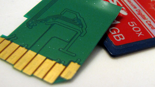
Next generation memory

Flash memory remains the dominant form of non-volatile (that is, preserving information in the absence of electric current) memory due to its wide use in solid-state drives (SSD) and the usual USB flash drives. But, despite its popularity and widespread use, the technology still remains problematic, especially if the production rate falls below the 30nm process - the speed of flash memory decreases. In addition, a limited number of write-erase cycles and a relatively low recording speed (in milliseconds). Due to all these limitations, researchers have long been looking for an effective replacement for flash memory for the production of the above products.
At the moment there are several alternative developments that could well replace silicon flash memory, such as PRAM (phase-change RAM), FeRAM (ferroelectric RAM), MRAM (magnetoresistive RAM) and RRAM (resistance-change RAM). However, until today, scientists from various universities and companies have not been able to successfully apply the current technological standard in memory production using any of these technologies - either the mode switching mechanism or the platform itself loses its efficiency and speed at the “nano” level. Plus, none of these developments lack such important characteristics in commercial production as an increase in write-erase cycles (as compared to flash memory), long-term data storage in the absence of current, and high switching speed between read / write modes. It is the qualitative and quantitative growth of these indicators that is considered the main requirement in the development of the next-generation non-volatile memory.
')
And, not for fun, the researchers plan to replace this technology entirely. A joint group of scientists from Samsung and Korean Sejong University recently published a curious publication in the journal Nature Materials , describing the new RRAM production technology (resistance-change RAM is a technology that allows cells to change the voltage so that its state changes from low resistance (high conductivity) to high resistance (low conductivity)) of tantalum oxide (TaO x ), which in tests showed a huge advantage over existing technologies, beating the results in almost all points.
The devices based on RRAM work as follows: with sufficient voltage, the material functioning under normal conditions as an insulator (high resistance state) switches to the low resistance state. The microcircuit itself, whose structure is multi-layered (sandwich), sits on the main layer of tantalum oxide (TaO 2-x ), on which a thinner layer of oxide (Ta 2 O 5-x ) is applied, acting as an insulating layer surrounded by platinum electrodes. This configuration, known as MIMB (metal-insulator-base-metal) is an insulator that can switch to a high conductivity state by changing its configuration to MMBM (metal-metal-base-metal). Interesting, isn't it?
Actually, the nature of the process of such switching has not yet been fully studied, but the authors of the study believe that laying high-conductive filaments extending through the layer of Ta 2 O 5-x oxide will cause oxygen ions to move at high enough voltages. the result of the redox process.
So, in the insulating (MIMB) state, what is between the platinum electrode and tantalum oxide forms a metal-semiconductor transition, also known as the Schottky Barrier , while in the highly conductive (MMBM) state, the same forms ohmic contact. The main difference between the two is that the current profile (depending on the voltage) is linear and symmetrical for an ohmic contact, but for the Schottky Barrier it is non-linear and asymmetric. The presence of the barrier is also advantageous, because does not allow wandering current through an array of multiple devices, which is important to ensure high density data storage.
The result of the above manipulations is memory, which, with a 30nm production process and a current of 50 microamperes (which is lower than the requirements of one of the alternative technologies - PRAM), beats the current flash memory figures. It was shown 10 12 (in today's flash memory, this figure varies between 10 4 -10 6 ) write-erase cycles with a switching time of 10 nanoseconds and an information storage period of 10 years at a temperature of 85 degrees Celsius. This is quite a serious leap forward, compared to the flash memory that is so common today. Plus, it is more stable and functions without problems in a vacuum.
It is likely that all this is too sweet and smooth to be true. It is immediately worth mentioning that the tests were carried out under laboratory conditions on a plate that can fit 64 bits of information (in this terminology, this is 64 memory modules). Before the market can appear gigabyte devices made by RRAM-technology, it will take several more years.
In the entire semiconductor industry, in order to start mass production, you need to make changes to the nanolithography process, but in this particular case, you will have to fully understand the mechanism for switching resistance states. But what the researchers showed as a result is impressive. If the RRAM is brought to mind, it can be used as a universal memory, suitable for both information storage and production of RAM.
For help with chemical formulas, thank you lesch
Nature Materials via ArsTechnica
Source: https://habr.com/ru/post/124155/
All Articles