Making home chips - steps 0 and 1
 In this article I will talk about the beginning of my work on a completely reckless task: the ultimate goal is to get a working chip according to “thick” norms (5-10µm) at home. This is not the first of April and I'm not crazy, it's just my hobby.
This idea arose not now and for good reason. Since childhood, I wanted to be a gas welder, and ... make chips. And if on the first point I quickly managed to make a welding machine at home (butane-hydrogen / oxygen), then with the microcircuits it still didn’t add up. For a long time, all thoughts stayed on the fact that I didn’t know where to get the proper semiconductors of the required purity (and they stopped on picking powerful transistors), until the forum suggested that in principle, you can buy plates. Then I even stumbled upon a man who had been working on a similar task for 20 years , and eventually gave up. Perhaps, it was possible to give up and stop wasting time on silly dreams. But, once I saw a movie of a monstrously brilliant woman - Jeri Ellsworth - she was able to make separate field-effect transistors based on factory plates - and then I decided that it was time to tackle this problem more closely.
In this article I will talk about my current progress, but do not expect a quick continuation - the whole process can easily take a couple of years.
Step 0:
All books on the topic from local online stores were bought (just for 1 shelf), all available collections of digitized books were downloaded from torrents. Of course, there is a lot of theoretical information there, but from the practical side - much is covered with darkness. Even the old technical processes are not described in detail anywhere, and therefore have to try a lot. He also searched the Internet in search of local suppliers of all potentially necessary materials (silicon itself, photoresists, chemicals, gases). It has not yet been possible to find a local company that can manufacture aspherical optics from optical / quartz glass - but this will not be an obstacle in the coming year.
')
Step 1: Silicon
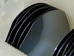
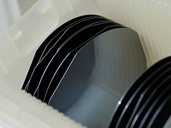 Monocrystalline silicon - the heart of the home chip. Growing up at home is real (by my crazy standards), but damn expensive. Therefore, I began to google local silicon producers - someone said that they had curtailed production and were only engaged in renting out premises, someone did not respond until I finally reached Therasil company - there I was finally able to buy everything I needed. The most important thing is the cut and polished plates of monocrystalline silicon doped in P and N type (on the right of the photo).
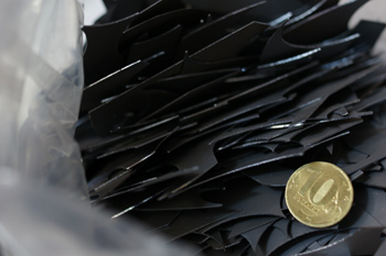 Next - a bunch of broken plates for training. I practiced splitting the plate into pieces (it turned out that all of them with the orientation of the 111 crystal lattice are split into triangles, not squares). Because they are not polished yet - I tried and polished - the failure is complete: the goy paste does not take silicon, diamond paste is needed. If over time it turns out to be polished, it will be possible to try to make solar cells (and from monocrystalline silicon they turn out to be quite effective).
 And finally - pieces of monocrystalline silicon. Those that are thick on the left are dirtier (but sufficiently clean for microcircuits), 2 thin ones on the right are ultrapure, much higher than the purity requirements of silicon for ordinary microcircuits. Of course, cutting them at home will not work (unless of course the diamond circular saw has stumbled) - just smash. We need to try to precipitate films of amorphous silicon by chemical (PE CVD SiH4) or physical (evaporation in a vacuum) way.
What are the next tasks?
- In the first place - the construction of the furnace at 1200 degrees for a small sample. Industrial furnaces under such a temperature in the apartment do not deliver, and they are worth it. Therefore I will try to heat the sample with halogen lamps with reflectors.
- Moving to a separate apartment: I was immediately expelled after seeing a bearded man in a gas mask and rubber gloves with a bunch of suspicious jars.
- Next - the necessary chemistry and photoresists - and you can try to do 1 transistor in the Jeri process.
What am I looking for and do not find it yet
First of all - this is information. I would like to have contacts of people who work in production - after all, I will collect all the rakes that technologists have collected over the past 50 years
Comments / opinions - in the studio.
Source: https://habr.com/ru/post/118534/
All Articles