Trigger Level Trigger
Synchronization is the main method of dealing with the competition of signals in digital circuits.
Unlike conventional asynchronous triggers, where, in accordance with the truth table, switching occurs at those times when the signals at the information inputs change, the synchronizing (clocked) triggers also have a control input (usually in the diagrams designated C). If the signal at this input accepts a resolving value, then the trigger works as asynchronous. If the signal at the clock input has a prohibitive value, then the trigger does not respond to changes in the signals at the information inputs and retains the information that it recorded during the last recording resolution.
Synchronization is of several types:
In this article we confine ourselves to the consideration of the first case.

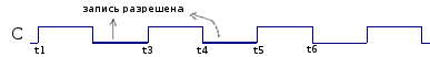
With the signal C = “1” (at the moments from t2n-1 to t2n) recording is allowed, with C = “0” - the storage mode.
')
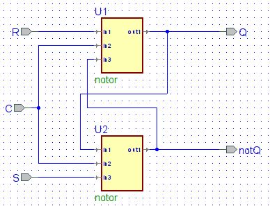
We illustrate this on an RS trigger with synchronization based on “or-not” elements (U1, U2) with three inputs.
The timing diagram of this trigger (without reading the delay on the valves):

In the “or-not” logic elements, the dominant signal is “1”, therefore, when the signal is C = 1, the signals at inputs R and S are blocked and the trigger will be in storage mode. When C = 0, the circuit operates as a normal RS trigger.
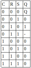
Truth table of this scheme:
With the signal C = “0” (at the moments from t2n to t2n + 1) recording is allowed, with C = “1” - the storage mode.
Imagine the operation of a clocked trigger based on a synchronizing E trigger based on “and-not” logic elements (U9, U3, U4, U1, U6, U5) and not (U10, U7, U8, U2).
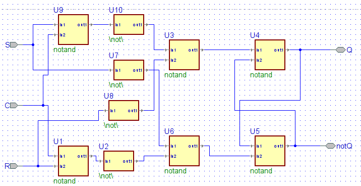
In the diagram, the “and-not” logical elements U9, U3 and the U10 inverter form the usual “and-not” logical element with three inputs. Similarly for U1, U2, U6.
Timing diagram of the scheme:
Since in the “and-not” elements the dominant signal is “0”, the incoming signals C = 0 block the R and S signals and therefore the trigger will retain its original state.
When C = 1, the flow of signals from the inputs R and S will be allowed and the circuit will work as a normal S trigger (switches to one state):
The signals C, S and notR go to inputs U3, and C, notS and R go to inputs U6. We obtain at the inputs of the RS trigger (U4 + U5) signals (not S || R) and (S || not R).
Truth table of this scheme:
Triggers with synchronization by signal level have one drawback - the change of input signals and their return to the initial position can occur during the resolution of the clocking signal, which will cause the output of the circuit to look through the input for a certain time interval.
Unlike conventional asynchronous triggers, where, in accordance with the truth table, switching occurs at those times when the signals at the information inputs change, the synchronizing (clocked) triggers also have a control input (usually in the diagrams designated C). If the signal at this input accepts a resolving value, then the trigger works as asynchronous. If the signal at the clock input has a prohibitive value, then the trigger does not respond to changes in the signals at the information inputs and retains the information that it recorded during the last recording resolution.
Synchronization is of several types:
- By the level of the clock signal
- By signal level “1”
- By signal level “0”
- On the front
- On the falling edge
- On the front edge
In this article we confine ourselves to the consideration of the first case.
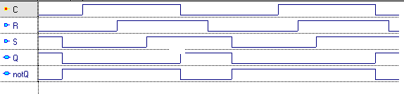
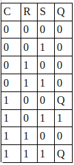
Synchronization of the signal level “1”
With the signal C = “1” (at the moments from t2n-1 to t2n) recording is allowed, with C = “0” - the storage mode.
')
We illustrate this on an RS trigger with synchronization based on “or-not” elements (U1, U2) with three inputs.
The timing diagram of this trigger (without reading the delay on the valves):
In the “or-not” logic elements, the dominant signal is “1”, therefore, when the signal is C = 1, the signals at inputs R and S are blocked and the trigger will be in storage mode. When C = 0, the circuit operates as a normal RS trigger.
Truth table of this scheme:
Synchronization of the signal level “0”
With the signal C = “0” (at the moments from t2n to t2n + 1) recording is allowed, with C = “1” - the storage mode.
Imagine the operation of a clocked trigger based on a synchronizing E trigger based on “and-not” logic elements (U9, U3, U4, U1, U6, U5) and not (U10, U7, U8, U2).
In the diagram, the “and-not” logical elements U9, U3 and the U10 inverter form the usual “and-not” logical element with three inputs. Similarly for U1, U2, U6.
Timing diagram of the scheme:
Since in the “and-not” elements the dominant signal is “0”, the incoming signals C = 0 block the R and S signals and therefore the trigger will retain its original state.
When C = 1, the flow of signals from the inputs R and S will be allowed and the circuit will work as a normal S trigger (switches to one state):
The signals C, S and notR go to inputs U3, and C, notS and R go to inputs U6. We obtain at the inputs of the RS trigger (U4 + U5) signals (not S || R) and (S || not R).
Truth table of this scheme:
Triggers with synchronization by signal level have one drawback - the change of input signals and their return to the initial position can occur during the resolution of the clocking signal, which will cause the output of the circuit to look through the input for a certain time interval.
Source: https://habr.com/ru/post/115690/
All Articles