The beginning of a new era
See what the matter is ...
Improvement of semiconductor technologies cannot last indefinitely - once again I want to return to a series of articles ( 1 | 2 | 3 ) about the production of processors, or rather, to post about the problems of this production. Any technology sooner or later loses its relevance, no matter how useful it is ... so one day the limit of reduction in the size of transistors and technical process will come, the imagination of the creators of new materials for the production of systems will end, and Moore's law (in the classic formulation of transistors) will become irrelevant. And when this "dead end" comes, the most interesting will begin - humanity will suffer in search of alternative technologies. In other matters, about the torment, I was probably in a hurry - it’s almost obvious that luminous electrons will be replaced by a luminous flux, and instead of copper (silver and gold) wires there will be some kind of optical medium. Yes, I hurried up, because the first attempts to create optoelectronic (combining optical and electronic technologies) systems were made almost a century ago, although under the influence of a harsh reality, everything was somewhat delayed.
')

Why did semiconductor electronics suddenly become “bad”? In fact, it did not become bad, just the electron is good, but the photon is better. What is the electric current, which today is in any technique? If you believe the school course of physics, then this is an orderly movement of charged particles ... which is one of the main problems. Pruschky electrons like tanks in a conductor are rather impractical - at least a significant part of their energy is lost, being released as heat and electromagnetic radiation, although this is not the only minus.
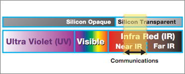
With light, everything is different - information in the form of a light beam can be transmitted at tremendous speed (here I mean throughput) and at least gigantic distances, while the losses will be minimal. Moreover, the processing of such information can be carried out directly during its transmission and almost without energy consumption - it is possible for a certain algorithm to pile up a complex system of lenses, light filters and other optical things that the incoming light beam at the output will transform into properly processed information.
The benefits of optical computing do not end there. You can add an extremely high degree of parallelization in the transmission and processing of data (due to simultaneous work with waves of different lengths), less power consumption, complete indifference to electrical noise and difficulty in intercepting data (since nothing is radiated to the surrounding space; still doctors and environmentalists finally sleep well). I wonder why all this expanse still does not displace semiconductor electronics? There is a whole bunch of correct answers to this question, which, in sum, lead to what we have now.
To make optical analogues of basic semiconductor elements is not a problem - it is much more difficult to make it all work, and to do it correctly and quickly. Indeed, ideally, to build an optical computer, one would have to abandon the classical architecture of von Neumann, and therefore one of its main principle, the principle of binary coding — sequences of zeros and ones may become irrelevant (although they could easily be transmitted by light pulses). It will be much more efficient to work with two-dimensional images - all this will increase the parallelism of computations by orders of magnitude (I remind you that “MHz-era” has already passed, and at the moment the performance of the same processors is growing mainly only due to parallelization of computations) and will enable to process even the largest data volumes - performance gains can be up to 10x or even 20x.
But ... but how in this case is it trivial to start working? ) Even if you perfectly master the skills of working on a regular computer, then you will have to learn to “walk again” with optics. How to live with a fundamentally different information structure, how and where to enter some data, how and where to get the results of calculations? It’s not so easy to translate the data of the usual modern look into the format required by the optical computer ... However, what I worry about is that even if optical computers appear in the foreseeable future, they will not be intended for home use the first time. But still, I still have more questions than answers.
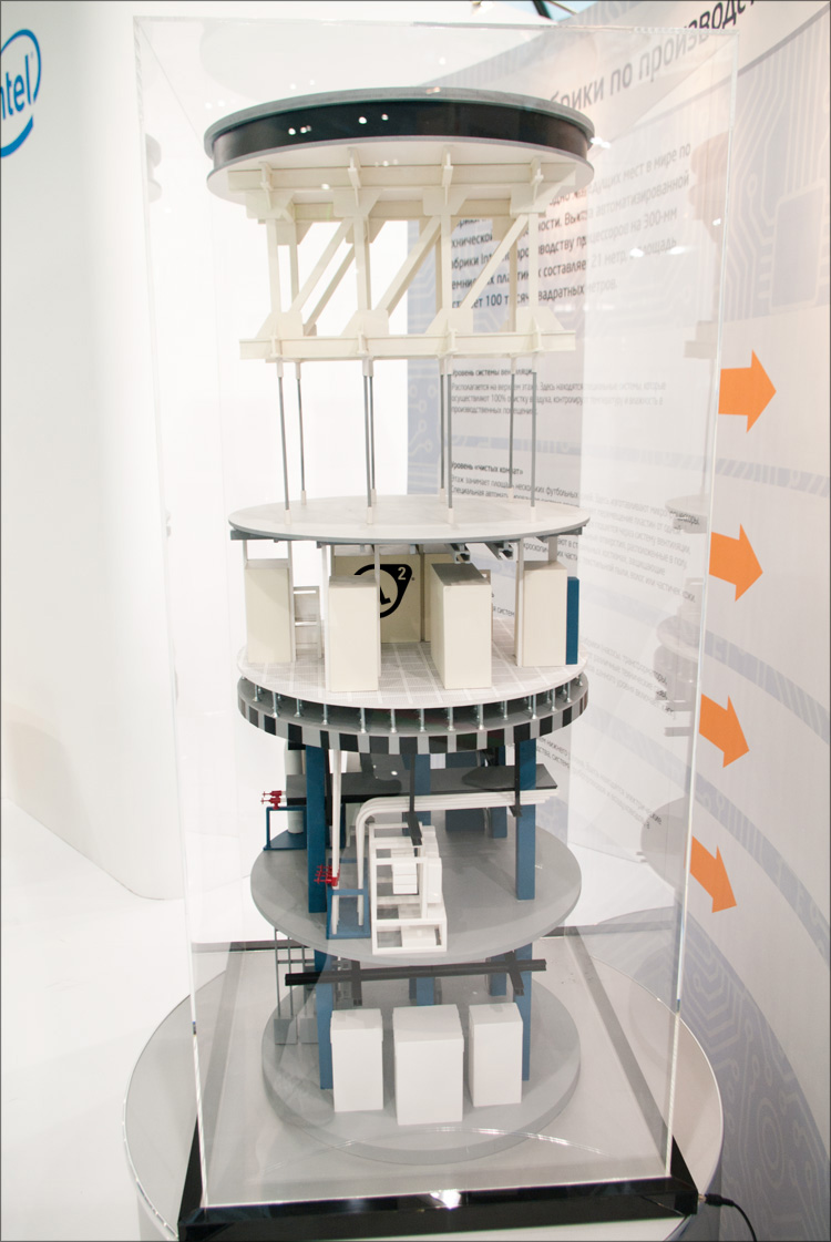
The layout of one of the buildings of the Intel factory for the production of processors
We must not forget about the cubic meters of money - apparently, it is now more profitable to build factories (capable of working on modern technological processes such as 22 or even 16 nm) worth several billion dollars, rather than producing fairly “simple” optical computers . Therefore, the best that in the near future shines us with friendly photons is a symbiosis of two epochs, that is, the usual semiconductor electronics complementing optics (and therefore, significantly limiting all its advantages). Examples of such solutions began to appear in the year since 1990 - it was then that the forge of Nobel laureates in the face of the research center Bell Labs created the first working prototype of an optoelectronic computer. The processor is based on two-dimensional matrices of bistable semiconductor elements with sets of quantum wells and electro-optical properties. The elements were illuminated by a semiconductor laser (the radiation power was 10 mW, the wavelength was 850 nm) through Dammen's holographic grating — after passing light through one diode, a current appeared in the circuit, which led to a voltage drop across the grating structure and an increase in light transmission through the second structure. Thus, feedback arose and a set of elements formed logical cells OR-NOT, OR-AND, etc. A little later, similar computers began to appear in other places, usually connected with the military industry, aviation, space, etc.
The basis of other devices became two-dimensional matrices and everything worked on vector-matrix logic, and this was done quite revealingly - the same 32-bit ROCC-processor DOC-II (Digital Optical Computer) from OptiComp performed about 1000 binary operations per second. The comparison will become clearer if you imagine that this thing was able to search a text word in text documents at a speed of 80,000 pages per second, that is, for some instant about 400 million (!) Characters were processed.

DOC-II optical processor
Speaking in the present tense, now there is only one commercial product of this kind in the whole world - the hybrid chip EnLight256 from the Israeli company Lenslet , capable of performing up to 8 × 10 12 (8 teraop) operations per second and processing up to 15 streams of HD video in real time. In this optical processor, data is simultaneously received from 256 optical inputs - the rays of 256 lasers are added or multiplied when they illuminate a special matrix (spatial light modulator 256x256; the size of the processor itself is 15x15 cm). And the optical output signals of the result of the calculations are read by an array of 256 light detectors ... it is obvious that such structures are not intended for ordinary "home" use, so do not expect a review in the near future) Of non-commercial projects, there are now prototypes of optical processors made on "normal »Factories with 65 and even 32nm technology, but everything is not so simple with them.
The first radio tubes appeared about a century ago and made a revolution. Relatively soon, they were replaced by semiconductors, who still run the show ... so that the next revolutionary revolution cannot be avoided, but you need to understand that this process is not fast. Big tasks need to be solved gradually, breaking them down into subtasks - before creating optical processors, it would be nice to create the infrastructure, to “fill my hand” in simpler conditions. What, in fact, does the company in whose blog you read this article. The development of silicon photonics, Intel is far from the first day, and in 2015 the mass introduction of new technologies is already planned. Although what is there in 2015, if everything started a couple of years ago.

I'm talking about the fall of 2009, when Intel introduced the technology for transmitting data via optical fiber to the public, with the interesting code name Intel Light Peak . The development was intended to connect two computers at a distance of up to 100 meters and at a speed of up to 10 Gbit / s. Maybe these numbers do not surprise you, but it is important to note something different here - in fact, this technology became a light at the end of the tunnel, because the first thing to do before the start of the “new era” is to abandon metallic conductors. And to do this wherever possible - not only from computer to computer, but even inside the processor. But then later it will be possible to take up the program "optical computer in every home." But Intel’s Light Peak strategy in I / O is not limited to just one interface ...
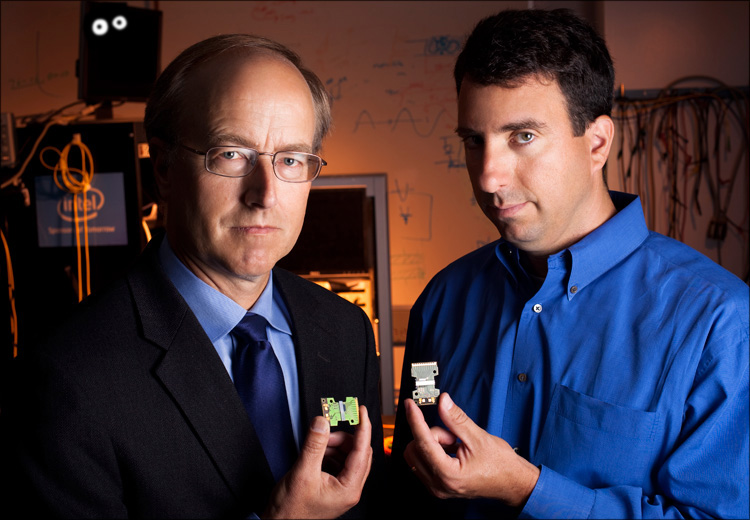
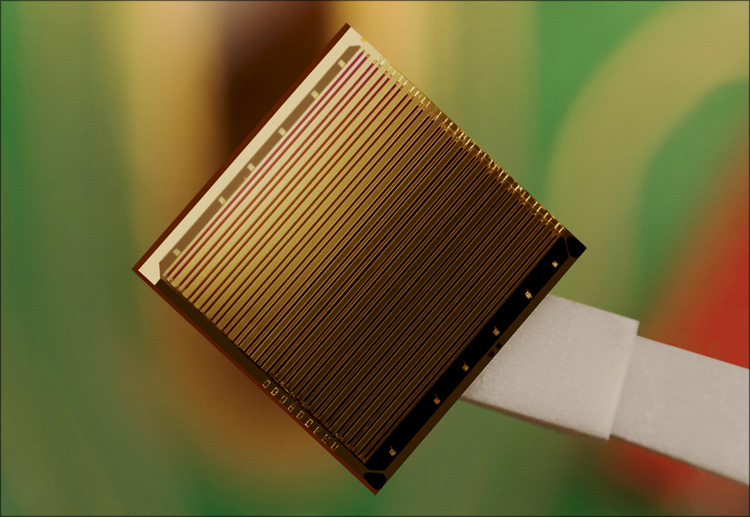
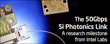
And how do you, for a start, the speed of 50 Gbit / s? It is this speed (in the first prototype) that implies another technology, announced last summer and called Intel Silicon Photonics Link . Despite the fact that technologies are developing separately from each other, here the principle of operation is in many ways similar to the Intel Light Peak. At the heart of the work - silicon transmitter and chip receiver; both with all the necessary unique components from Intel, including the first hybrid silicon-laser chip ( HSL ), as well as the high-speed optical modulators and photo sensors announced in 2007.
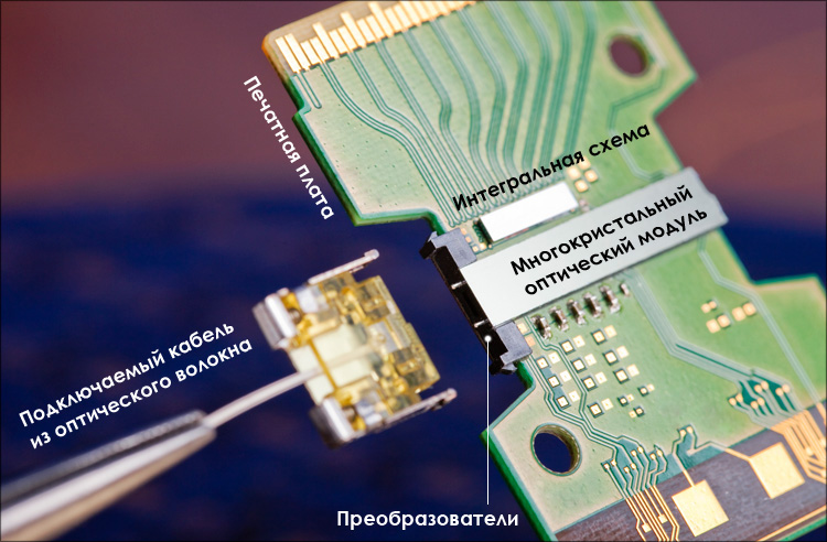
Transmitting chip and receiver chip

Photo Detector Chip
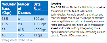
The transmitting chip consists of four lasers - their light rays enter the optical modulator, which encodes data at a speed of 12.5 Gbit / s. After that, the rays are combined into a single fiber with a bandwidth of 50 Gbit / s. At the other end of the channel, the receiver chip splits the beams and sends them to photodetectors that convert the data into electrical signals.
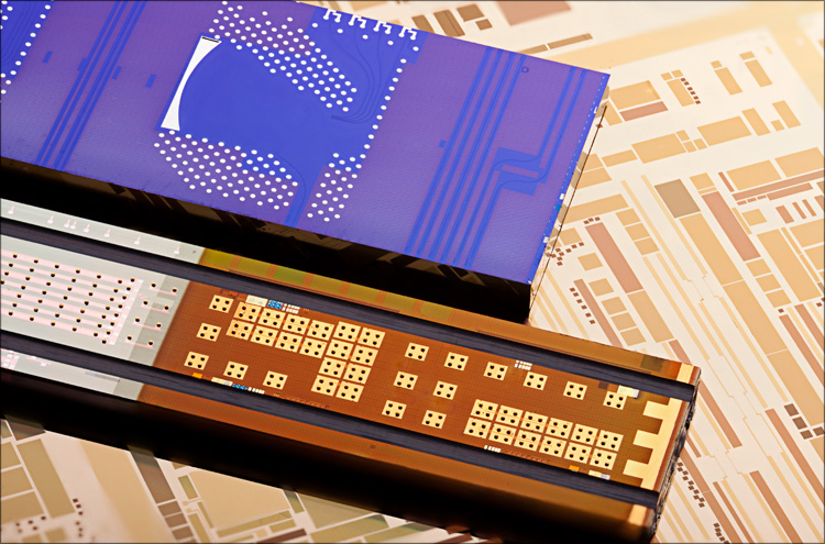
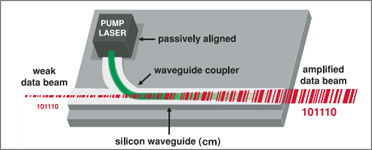
HSL (Hybrid Silicon Laser) - Hybrid Silicon Chip Laser
Where might this speed be needed? It is clear that at first it will be some kind of industrial scenarios, such as connecting highways between servers or even data centers. But when the technology becomes more accessible, I’m giving a tooth that devices with QuadHD-resolution (2160p) and 3D support (at least 120 Hz) will be in fashion - so with a color depth of 48 bits, the technology will barely suffice) On the other hand , nothing prevents it from growing, increasing the speed of the modulator and the number of lasers on a chip.
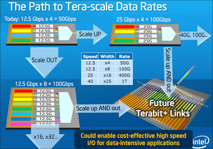
According to the researchers, Intel Silicon Photonics Link technology will make it possible in the future to transfer data at speeds up to 1 Tbit / c - it’s even scary to imagine what prospects will open at such speeds!
I think all of you know that on February 24, 2011, the announcement of Intel Thunderbolt technology took place, which “coincidentally” on the same day coincided with the announcement of Apple's new Macbook Pro notebooks. Two giants decided to combine their efforts, with the result that a new interface appeared, which has much in common with Intel Light Peak.

 Intel Thunderbolt (translated as “lightning strike”) in new MacBooks — an input / output interface for various peripheral devices that is based simultaneously (within one connecting cable up to 3 meters long) using two protocols: Displayport for transmitting images with a resolution of over 1080p and up to eight audio channels, and PCI-Express 2.0 4x for high-speed data transfer. In fact, an external PCI Express connector appeared on board the new MacBooks, which many users and even manufacturers dreamed of. The existing equipment with a DisplayPort interface is compatible with the new connector, and the common connectors imply connecting several devices one after the other (a hot connection is supported).
The theoretical data transfer rate of Intel Thunderbolt technology is up to 10 Gbit / s, but so far in practice there are more modest numbers - up to 800 MB / s (~ 6 Gbit / s). But not bad either!
In fact, Intel Light Peak is a universal technology that can be based on any protocol, and Thunderbolt is just one interpretation. That is, it turns out that the new technology is quite capable of competing with many wired interfaces (such as SCSI, SATA, FireWire, Ethernet, HDMI, and even USB 3.0) even without electronic-optical and opto-electronic converters, with copper instead of optics. What will be next? Most interesting.
I hope I could convince you that progress does not stand still. I will say more - according to historical standards, quite a bit of time must pass before the moment when great changes begin in the computer world, so we can say that we are very close to the beginning of a new era. In an interesting time we live, comrades! However, I do not know about you, but I was pleased to dream)
If, after reading the article, there remains an overwhelming desire to learn new technologies, their operating principles and technical features, then you can start with this:
50G Silicon Photonics Link Intel Advances Silicon Photonics
3.85 MB, in English 434 Kb, in English
Intel Silicon Photonics Link Hybrid silicon laser
219 Kb, in English 1.43 Mb, in English

Continuous silicon laser Optical transceivers
167 KB, in English 1.52 MB, in English

 Soon there will be an interesting series of articles in the company's blog - do not miss it!
Improvement of semiconductor technologies cannot last indefinitely - once again I want to return to a series of articles ( 1 | 2 | 3 ) about the production of processors, or rather, to post about the problems of this production. Any technology sooner or later loses its relevance, no matter how useful it is ... so one day the limit of reduction in the size of transistors and technical process will come, the imagination of the creators of new materials for the production of systems will end, and Moore's law (in the classic formulation of transistors) will become irrelevant. And when this "dead end" comes, the most interesting will begin - humanity will suffer in search of alternative technologies. In other matters, about the torment, I was probably in a hurry - it’s almost obvious that luminous electrons will be replaced by a luminous flux, and instead of copper (silver and gold) wires there will be some kind of optical medium. Yes, I hurried up, because the first attempts to create optoelectronic (combining optical and electronic technologies) systems were made almost a century ago, although under the influence of a harsh reality, everything was somewhat delayed.
')
Why did semiconductor electronics suddenly become “bad”? In fact, it did not become bad, just the electron is good, but the photon is better. What is the electric current, which today is in any technique? If you believe the school course of physics, then this is an orderly movement of charged particles ... which is one of the main problems. Pruschky electrons like tanks in a conductor are rather impractical - at least a significant part of their energy is lost, being released as heat and electromagnetic radiation, although this is not the only minus.
With light, everything is different - information in the form of a light beam can be transmitted at tremendous speed (here I mean throughput) and at least gigantic distances, while the losses will be minimal. Moreover, the processing of such information can be carried out directly during its transmission and almost without energy consumption - it is possible for a certain algorithm to pile up a complex system of lenses, light filters and other optical things that the incoming light beam at the output will transform into properly processed information.
The benefits of optical computing do not end there. You can add an extremely high degree of parallelization in the transmission and processing of data (due to simultaneous work with waves of different lengths), less power consumption, complete indifference to electrical noise and difficulty in intercepting data (since nothing is radiated to the surrounding space; still doctors and environmentalists finally sleep well). I wonder why all this expanse still does not displace semiconductor electronics? There is a whole bunch of correct answers to this question, which, in sum, lead to what we have now.
Oxygen free copper is canceled?
To make optical analogues of basic semiconductor elements is not a problem - it is much more difficult to make it all work, and to do it correctly and quickly. Indeed, ideally, to build an optical computer, one would have to abandon the classical architecture of von Neumann, and therefore one of its main principle, the principle of binary coding — sequences of zeros and ones may become irrelevant (although they could easily be transmitted by light pulses). It will be much more efficient to work with two-dimensional images - all this will increase the parallelism of computations by orders of magnitude (I remind you that “MHz-era” has already passed, and at the moment the performance of the same processors is growing mainly only due to parallelization of computations) and will enable to process even the largest data volumes - performance gains can be up to 10x or even 20x.
But ... but how in this case is it trivial to start working? ) Even if you perfectly master the skills of working on a regular computer, then you will have to learn to “walk again” with optics. How to live with a fundamentally different information structure, how and where to enter some data, how and where to get the results of calculations? It’s not so easy to translate the data of the usual modern look into the format required by the optical computer ... However, what I worry about is that even if optical computers appear in the foreseeable future, they will not be intended for home use the first time. But still, I still have more questions than answers.
The layout of one of the buildings of the Intel factory for the production of processors
We must not forget about the cubic meters of money - apparently, it is now more profitable to build factories (capable of working on modern technological processes such as 22 or even 16 nm) worth several billion dollars, rather than producing fairly “simple” optical computers . Therefore, the best that in the near future shines us with friendly photons is a symbiosis of two epochs, that is, the usual semiconductor electronics complementing optics (and therefore, significantly limiting all its advantages). Examples of such solutions began to appear in the year since 1990 - it was then that the forge of Nobel laureates in the face of the research center Bell Labs created the first working prototype of an optoelectronic computer. The processor is based on two-dimensional matrices of bistable semiconductor elements with sets of quantum wells and electro-optical properties. The elements were illuminated by a semiconductor laser (the radiation power was 10 mW, the wavelength was 850 nm) through Dammen's holographic grating — after passing light through one diode, a current appeared in the circuit, which led to a voltage drop across the grating structure and an increase in light transmission through the second structure. Thus, feedback arose and a set of elements formed logical cells OR-NOT, OR-AND, etc. A little later, similar computers began to appear in other places, usually connected with the military industry, aviation, space, etc.
The basis of other devices became two-dimensional matrices and everything worked on vector-matrix logic, and this was done quite revealingly - the same 32-bit ROCC-processor DOC-II (Digital Optical Computer) from OptiComp performed about 1000 binary operations per second. The comparison will become clearer if you imagine that this thing was able to search a text word in text documents at a speed of 80,000 pages per second, that is, for some instant about 400 million (!) Characters were processed.
DOC-II optical processor
Speaking in the present tense, now there is only one commercial product of this kind in the whole world - the hybrid chip EnLight256
from the Israeli company Lenslet , capable of performing up to 8 × 10 12 (8 teraop) operations per second and processing up to 15 streams of HD video in real time. In this optical processor, data is simultaneously received from 256 optical inputs - the rays of 256 lasers are added or multiplied when they illuminate a special matrix (spatial light modulator 256x256; the size of the processor itself is 15x15 cm). And the optical output signals of the result of the calculations are read by an array of 256 light detectors ... it is obvious that such structures are not intended for ordinary "home" use, so do not expect a review in the near future) Of non-commercial projects, there are now prototypes of optical processors made on "normal »Factories with 65 and even 32nm technology, but everything is not so simple with them.Intel Light Peak
The first radio tubes appeared about a century ago and made a revolution. Relatively soon, they were replaced by semiconductors, who still run the show ... so that the next revolutionary revolution cannot be avoided, but you need to understand that this process is not fast. Big tasks need to be solved gradually, breaking them down into subtasks - before creating optical processors, it would be nice to create the infrastructure, to “fill my hand” in simpler conditions. What, in fact, does the company in whose blog you read this article. The development of silicon photonics, Intel is far from the first day, and in 2015 the mass introduction of new technologies is already planned. Although what is there in 2015, if everything started a couple of years ago.
I'm talking about the fall of 2009, when Intel introduced the technology for transmitting data via optical fiber to the public, with the interesting code name Intel Light Peak . The development was intended to connect two computers at a distance of up to 100 meters and at a speed of up to 10 Gbit / s. Maybe these numbers do not surprise you, but it is important to note something different here - in fact, this technology became a light at the end of the tunnel, because the first thing to do before the start of the “new era” is to abandon metallic conductors. And to do this wherever possible - not only from computer to computer, but even inside the processor. But then later it will be possible to take up the program "optical computer in every home." But Intel’s Light Peak strategy in I / O is not limited to just one interface ...
Intel Silicon Photonics Link
And how do you, for a start, the speed of 50 Gbit / s? It is this speed (in the first prototype) that implies another technology, announced last summer and called Intel Silicon Photonics Link . Despite the fact that technologies are developing separately from each other, here the principle of operation is in many ways similar to the Intel Light Peak. At the heart of the work - silicon transmitter and chip receiver; both with all the necessary unique components from Intel, including the first hybrid silicon-laser chip ( HSL ), as well as the high-speed optical modulators and photo sensors announced in 2007.
Transmitting chip and receiver chip
Photo Detector Chip
The transmitting chip consists of four lasers - their light rays enter the optical modulator, which encodes data at a speed of 12.5 Gbit / s. After that, the rays are combined into a single fiber with a bandwidth of 50 Gbit / s. At the other end of the channel, the receiver chip splits the beams and sends them to photodetectors that convert the data into electrical signals.
HSL (Hybrid Silicon Laser) - Hybrid Silicon Chip Laser
Where might this speed be needed? It is clear that at first it will be some kind of industrial scenarios, such as connecting highways between servers or even data centers. But when the technology becomes more accessible, I’m giving a tooth that devices with QuadHD-resolution (2160p) and 3D support (at least 120 Hz) will be in fashion - so with a color depth of 48 bits, the technology will barely suffice) On the other hand , nothing prevents it from growing, increasing the speed of the modulator and the number of lasers on a chip.
According to the researchers, Intel Silicon Photonics Link technology will make it possible in the future to transfer data at speeds up to 1 Tbit / c - it’s even scary to imagine what prospects will open at such speeds!
 Intel thunderbolt
I think all of you know that on February 24, 2011, the announcement of Intel Thunderbolt technology took place, which “coincidentally” on the same day coincided with the announcement of Apple's new Macbook Pro notebooks. Two giants decided to combine their efforts, with the result that a new interface appeared, which has much in common with Intel Light Peak.
Intel Thunderbolt (translated as “lightning strike”) in new MacBooks — an input / output interface for various peripheral devices that is based simultaneously (within one connecting cable up to 3 meters long) using two protocols: Displayport for transmitting images with a resolution of over 1080p and up to eight audio channels, and PCI-Express 2.0 4x for high-speed data transfer. In fact, an external PCI Express connector appeared on board the new MacBooks, which many users and even manufacturers dreamed of. The existing equipment with a DisplayPort interface is compatible with the new connector, and the common connectors imply connecting several devices one after the other (a hot connection is supported).The theoretical data transfer rate of Intel Thunderbolt technology is up to 10 Gbit / s, but so far in practice there are more modest numbers - up to 800 MB / s (~ 6 Gbit / s). But not bad either!
In fact, Intel Light Peak is a universal technology that can be based on any protocol, and Thunderbolt is just one interpretation. That is, it turns out that the new technology is quite capable of competing with many wired interfaces (such as SCSI, SATA, FireWire, Ethernet, HDMI, and even USB 3.0) even without electronic-optical and opto-electronic converters, with copper instead of optics. What will be next? Most interesting.
| It is noteworthy that the name Thunderbolt is quite common. For example, from the latter, the Thortech company (a subsidiary of GeIL) released the eponymous series of powerful power supplies, and HTC officially presented the namesake communicator with LTE for Verizon at CES2011. In the game Mafia2, there was a Smith Thunderbolt car, and in the first Quake it was one of the most powerful weapons (it was also called Lighting Gun). And if you move away from the IT-sphere, you can not fail to mention about two legendary American aircraft - the Republic P-47 Thunderbolt fighter-bomber and the Fairchild Republic A-10 Thunderbolt II attack aircraft. Such he is different, this bolt!  |
Harsh reality
I hope I could convince you that progress does not stand still. I will say more - according to historical standards, quite a bit of time must pass before the moment when great changes begin in the computer world, so we can say that we are very close to the beginning of a new era. In an interesting time we live, comrades! However, I do not know about you, but I was pleased to dream)
If, after reading the article, there remains an overwhelming desire to learn new technologies, their operating principles and technical features, then you can start with this:
50G Silicon Photonics Link Intel Advances Silicon Photonics3.85 MB, in English 434 Kb, in English
Intel Silicon Photonics Link Hybrid silicon laser219 Kb, in English 1.43 Mb, in English
Continuous silicon laser Optical transceivers167 KB, in English 1.52 MB, in English
Soon there will be an interesting series of articles in the company's blog - do not miss it!Source: https://habr.com/ru/post/115638/
All Articles