Prospects for the development of central processing units
Seventy years ago, in 1941, the first programmable computer was created. Since then, much water has flowed, and now computers surround us everywhere. Many aspects of the device computers have evolved greatly, many, by contrast, have not changed in essence. In particular, the very principle of operation of the central processors — the algorithmic model — has never changed and probably will never change. The physical limitations of this model are well understood, and accordingly, the limit of development of central processors in the sense of their speed is clearly visible. Technologically, this ceiling is still quite far: several decades of development and several orders of speed. But this should not prevent us from seriously thinking about what kind of processors will be at the threshold of their speedy development.
It is possible to make predictions in this area that the possible paths of development are strictly dictated by fundamental physical limitations: the finite speed of light, the laws of thermodynamics, and the restriction on the minimum size of theelements — they cannot be smaller than a molecule.
devices, from microwaves to robotic production lines and from mobile phones to spacecraft. In particular, it is the controlling role that he plays in laptops, desktop workstations, and game consoles — devices called consumer computers.
There are several essentially different models of computation, so the future AVMs may be arranged in a completely unforeseen way. However, the computer as a control device in any case must contain an executive unit (central processor), and the device of this unit is rigidly fixed by its functions: it must be able to
- issue successive instructions to other devices and
- to make a choice of a further program of action depending on the prevailing conditions.
These two requirements automatically assume a device model called “relaxed sequential execution” in English or “algorithmic model” in the Russian-language tradition. This model, unlike many others, has no quantum analogue, since quantum computations are fundamentally reversible, and making a choice is fundamentally irreversible. It is about this model that will be discussed in the following two parts of the article.
')
For the sake of completeness, here is a list of all scalable hardware models of calculations known for this moment:
- an algorithmic model, that is, (conditionally) step-by-step execution of instructions (“conditionally” means that parallel execution of independent instructions is allowed);
- stream vector calculations and their naturalgeneralization - quantum pipelines;
- cellular / network automata and their naturalgeneralization - quantum automata.
Currently, in practice, with the exception of the sequential execution model, only streaming vector calculations are used: on consumer computers in specialized coprocessors for three-dimensional graphics (GPU), as well as in their high-power counterparts (GPGPU) on computing stations for numerical simulations and processing large data arrays . The central processor delegates some specific tasks to the streaming processor, however, only he himself performs the controlling functions. With the development of quantum computing, this state of affairs is unlikely to change: quantum conveyors and automata will only be additions to the central processor, but not its replacement.
In digital electronics around us, transistors are used as switches, and tracks are made of conductors.
§ 2.1. Signal transmission
 Binary digital electronics uses voltage to encode the signal. A track carries a “zero” signal, if a potential is applied to it
 (U 0 ± ε) , and if a potential is applied to it (U 1 ± ε) , then it carries a “one” signal. The base levels U 0 and U 1 are chosen so that (U 0 + ε) <(U 1 - ε), where ε is an error that is unavoidable for technical reasons. The transition from one state to another is a stop or, on the contrary, the acceleration of a huge number of electrons in a conductor. Both of these processes take a lot of time and are inevitably associated with large energy losses.
There are alternatives to digital electronics devoid of this drawback: a constant stream of electrons (so-called spintronics) or photons (so-called photon logic) can be started along the tracks, and the signal can be encoded using the polarization of this stream. Both electrons and photons moving along a one-dimensional waveguide can exist in exactly two orthogonal polarization states, one of which is declared zero, and the other one. What is better - photon logic or spintronics, is not yet clear:
- in both cases, the flow of particles flows with inevitable heat losses, however, these losses can be arbitrarily small;
- in both cases, the flow velocity is lower than the speed of light, however, it can be as close as possible to it;
- in both cases, complex techniques are required so that pickups, thermal noise and background radiation (random particles passing by) do not distort the signal.
In other words, the known physical limitations of both technologies are the same. Apparently, the best results will be given by combined technologies: transportation of photons wins at long distances and loses at short distances; however, working prototypes of adapters (in both directions) between the polarization of the photon and electron flux have already been developed. The ideal material for spintronic tracks is graphene: it provides excellent speed with very low heat loss. In addition, working prototypes of the following elements already exist:
- tracks, reliably preserving the polarization of the current at short and medium distances;
- memory cells capable of maintaining polarization and then forming a stream of stored polarization.
Information on graphene tracks:
2010-06: Mass fabrication of graphene nanowires. Georgia Institute of Technology.
2011-01: Researchers managed to generate a spin current in Graphene. City University of Hong Kong.
2011-02: Creating a pure spin current in graphene. City University of Hong Kong.
2011-02: Mass production-ready bottom-up of defect-free graphene nanoribbons. Max Planck Institute for Polymer Research in Mainz.
§ 2.2. Switches
 Used in digital electronics, the transistor is a device with three contacts, working as follows:
- if a high potential is applied to the middle contact, then the extreme contacts are connected, the switch is in the “conductor” position;
- if a low potential is applied to the middle one, then the extreme contacts are open, the switch is in the “isolator” position.
At the moment, transistors consisting of one molecule have been successfully created and tested. Their speed and compactness almost reach the theoretical limit, but so far there are no technologies that would allow them to be mass produced and used. All modern digital electronics are made on the basis of metal oxide field-effect transistors (MOSFET). For several decades, manufacturers of microcircuits have only reduced the linear dimensions and power consumption of such transistors, however, industrial tests of some types of multi-current and non-transition transistors (BDT, JNT) have already been carried out. Such transistors will be able to provide an increase in performance of4-6 times. This transition will not require major changes in the process and is expected in the next 5–10 years.
For fundamental thermodynamic reasons, transistor-type switches cannot work effectively: effective must be conservative and reversible as a logical element. These conditions are satisfied by a symmetric switch, also called Fredkin's valve.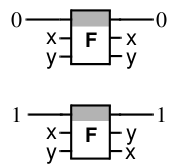 This device has two inputs In 1 , In 2 , two outputs Out 1 , Out 2 and
 pass -through track C (Control) . If C is in the “0” position, the inputs and outputs are connected directly: In 1 to Out 1 , In 2 to Out 2 ; if C is in the “1” position, the inputs and outputs are cross-connected: In 1 with Out 2 , In 2 with Out 1 . Most likely, the spin symmetric switches can be implemented in a single-molecular version, combining maximum compactness, speed and efficiency.
Both transistors and symmetric switches can be used to make logic circuits of any complexity, but symmetric switches are much more economical. For example, to clone a signal and the logical operations “not”, “and”, “or”, “and not” and “should”, only one symmetric switch is required, “exclusive or”, “not or” and “not and” require two switches. To implement these operations on transistors, from 4 to 6 transistors are required:

 A fast one-digit adder (half adder) uses four symmetric switches (instead of 12 transistors) and ideally provides a significantly higher speed of operation than a transistor analog: its operating time is only 2τ, where τ is the signal passing time of one switch and one track. On more complex circuits, the compactness and speed gain of symmetric switches are even more pronounced. The multi-bit adder link (full adder) consists of dozens of transistors, while the implementation on symmetric switches requires from 4 (the most compact version) to 7 (the fastest option) switches:
A unique feature of symmetric switches is that they help to achieve maximum compactness and speed of operation of multiplexers and demultiplexers, which are very common constituent elements of processors. Unfortunately, symmetric switches become attractive only when using spintronics or photon logic. Electronics is doomed to use conventional transistors.
* The paragraph used materials and images from articles by Bruce, Thornton et al. , “Efficient Adder Circuits Based on a Conservative Reversible Logic” (Mississippi State University, Proc. IEEE Symposium on VLSI, 2002); Rentergem, de Vos , “Optimal Design of A Reversible Full Adder” (Universiteit Gent, International Journal of Unconventional Computing, 2005), as well as private correspondence. The image of the unmolecular transistor is taken from the corresponding press release on the website of Yale University.
§ 2.3. Conclusion
So, in the limit, the central processor of the future is likely to be a huge web, where the threads are made of graphene tape, conducting a polarized electron flow, and in the nodes there are miniature symmetric switches. At long distances, the signal will be recoded to light, delivered by photons and recoded back to the destination. A number of special tasks (in particular, search and sorting) will be performed by quantum conveyors and automata.
- the processor contains a certain number (for example, 16) of numbered memory cells (for example, 64 bits each), which are called operational registers;
- the processor is to process the contents of the registers in accordance with the program;
- the program is a sequence of instructions, for example:
- take values from registers No. 2 and No. 5 and record their sum in register No. 8;
- read in register No. 4 the value from the external memory cell with the address from register No. 6;
- send the number from register No. 12 to the external device NNN;
- the data and the programs themselves are stored in RAM, while the instructions of the programs are encoded with numbers and recorded in successive memory cells;
- the number of the cell, the instruction from which is being executed at the moment, is stored in a special register called the Instruction Pointer, which at the end of the execution is moved to the next memory cell.
For more than half a century since the emergence of this architecture, dozens of alternative arivetekture organizations for sequential execution have been proposed, but all of them are inferior to it in the performance ceiling. The performance ceiling is determined (due to the finiteness of the speed of light) by the linear dimensions of the critical part of the structure, and it is the classical register architecture that ensures the maximum locality of the computation from all the currently proposed sequential execution architectures. Accordingly, it is precisely this architecture that will preserve, apparently, in thefuture - at least a few more decades.
§ 3.1. Functional logical units
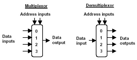
 The switches and tracks described in the first part are the “raw materials” for the production of functional logical units, such as an adder, multiplier, multiplexer and demultiplexer. Multiplexers and demultiplexers are devices that are similar to the sorting stations on the railway (see the illustration to the right). The input of the multiplexer receives n numbers ( a 1 .. a n ) and the control number m . The output is a number a m , that is, the
 m -th of n input numbers. The demultiplexer is a mirror analogue of the multiplexer: it transmits the incoming signal to the m -th out of n outputs.
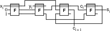
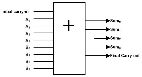
The task of the adder is to add the numbers supplied to it. The input of then- bit adder receives two numbers a and b for n bits plus a one-bit number c (0 or 1). The adder adds the incoming numbers and gives the result ( a + b + s ) . This is an ( n + 1) -bit number.
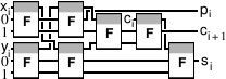
Functional-logical units do not immediately respond to changes in the arguments: the signal needs to go all the way from the beginning of the circuit to its end, taking into account the delays caused by passing through the switches and possible cycles in the circuit. For each functional logical unit in the design time is calculated. An extensive theory of designing functional-logical units with a minimum operation time has been developed. So, the simplest multi-digit adder that performs addition according to the image and similarity of addition to a column on paper requires for the operation time that grows linearly with the digit capacity. In the 1960s, accelerated transfer schemes were developed, reducing growth to logarithmic. The adder using them on symmetric switches is guaranteed to calculate the result for ⌈3 + log 2 (digit capacity) · τ, which is the theoretical speed limit. In the case of a 64-bit adder, a 15-fold acceleration is achieved, compared to a naive implementation. And the ingenious optimization of multiplication, division, calculation of trigonometric functions makes it possible sometimes to achieve acceleration hundreds of times.
§ 3.2. Operating units
An operationunit is a device that can perform instructions of a single type — for example, addition and subtraction. The basic element of the operating unit is a memory cell (the so-called instruction register) into which the instruction to be executed is written. Upon execution of the instruction, the unit clears this cell. The rest of the operational unit consists of a set of interconnected logical-unit instructions with each other and with the register. For example, consider an operating unit capable of performing instructions of the form “add up values from registers No. 2 and No. 5 and write the amount into register No. 8. "
We will need:
- the instruction register in which the summation operation code and the numbers of the operand registers are stored (2, 5 and 8 in the above command);
- adder;
- two multiplexers connected to the block of registers on the one hand and the inputs of the adder on the other: they select from the registers those two whose numbers are stored in the register instructions (No. 2 and No. 5 ) and serves the contents to the inputs of the adder;
- one demultiplexer that supplies the output of the adder to the inputs of the register in which it should be saved.
In modern processors, operating units can perform more than one action. For example, a block may contain, in addition to an adder, a multiplier. For technical implementation, it is enough to put a multiplier, framed by a demultiplexer and a multiplexer, in parallel with the adder, which choose to carry the signal through an adder or multiplier depending on the operation code stored in the instruction register.
§ 3.2.1. Organization of the operating cycle: synchronization, superscalarity, pipelining
The work of the processor is a repetition of the next cycle, during which information passes in a circle “registers → operating units → registers”:
- load the instructions to be executed into the operating units;
- wait for the results;
- save results to registers.
There are two approaches to the organization of the processor cycle: synchronous and asynchronous. In synchronous processors there is a signal conductor. When it changes (“the conductor wavers his wand”), the values issued by the operating units are saved to the registers, and the following instructions are given to the operating units. In asynchronous processors, there is no common signal conductor, and the operational units themselves report the readiness of the result. From the moment the task and the operands are ready, the block starts tracking the readiness of the result. At the end of the calculation, the block gives a go-ahead for saving the result and asks for the next task.
Synchronous processors have a fixed clockfrequency - the number of "sweeps of a conductor's stick" per second. The time between “sweeps” has to be chosen on the basis of the most pessimistic scenario. However, in practice, in the overwhelming majority of cases, the operation takes several times less time. Three factors affect the execution speed:
- the initial state of the operational block: if the instruction or part of the arguments is loaded in advance, part of the block comes to the desired state in advance;
- operand values: for example, multiplying short numbers takes a lot less time than multiplying long ones;
- background noise level: at a processor temperature of20 ° C, all operations proceed much faster than at a temperature of 90 ° C.
The synchronous approach cannot take into account all these factors; In addition, the dependence of the noise level on temperature is determined by the concentration of crystaldefects — a value that varies from instance to instance and increases as the processor ages. When calculating the processor clock frequency, one should proceed from the worst, that is, from a worn mediocre specimen operating at a temperature of 85–90 ° C. This fact is used by people who perform the so-called processor overclocking (“overclocking”): successful instances with sufficient cooling continue to work stably with a significant excess of the clock frequency set by the manufacturer.
Asynchronous processors begin the next operation as soon as the results of the previous one are ready. They have no such thing as a clock frequency, and their speed is always the maximum for these conditions: if you put hot coffee on an asynchronous processor, it slows down, if you pour it with liquidnitrogen, it accelerates. However, asynchronous circuitry due to its complexity is used today only in a small number of experimental asynchronous processors (starting with ILLIAC I in 1951 and ending with GA144 in 2010). In the future, it will probably be used more and more, since there is no other optimization area left.
For more than a decade several processors of each type have been installed in processors. Such processors are called superscalar. They can perform independentactions in parallel - for example, they can follow the instructions “c = a + b” and “d = a · b” in parallel. Another widely used optimization technique is the so-called “pipelining”: the instruction task is written into the operational blocks before the operands are ready, while the multiplexers and demultiplexers have time to arrive in the right state in advance, and the operation time is dramatically reduced. However, the maximum benefit from the use of pipelining can only be obtained on an asynchronous processor, since synchronous processors provide for the execution of each instruction in advance a fixed number of “wands of a conductor's stick”, and the benefits from the proactive loading of instructions into blocks are relatively small. If, in addition, separately monitor the readiness of each operand, on an asynchronous processor, you can get a gain in time not only by preloading instructions, but also by earlier readiness of one of the operands.Sometimes the instruction can work in general before all operands are ready - for example, if one of the operands is equal to zero, the multiplication will produce zero, without waiting for the second operand to be ready.
The only effective way to separately control the availability ofoperands is one-time use of registers. This term means that during the work of each subprogram, writing to each register occurs only once (the values are never overwritten). At the end of the procedure, all used registers are reset back to the empty state. This ensures simplicity of operand readiness check: the operand is ready as soon as the register containing it is non-empty. A straightforward implementation of separate readiness control requires a huge number of registers, but in practice this is not required: you can emulate a large number of logical registers, in fact, bypassing a small number of hardware registers.
§ 3.3. Control blocks and interrupt block
The distribution of tasks by operational blocks in accordance with the program recorded in the RAM is handled by the control unit. It loads the program's commands from RAM, decodes them, and, in decoded form, sends free operational blocks to the registers. In addition, it executes transition and branching instructions, that is, it selects one of the program branches depending on the value of some operational register. There can be several control blocks in the processor, which allows you to execute several programs in parallel.
CPUs not only execute programs, but also respond to hardware requests. Hardwarerequest - This is a signal supplied by external devices to dedicated processor inputs. For example, when you click on the mouse button, the processor is asked to handle this event. The processing of hardware requests is done by the interrupt block. When a request arrives, the interrupt block searches for a free control block and sends an order to execute the handler program. If there are no free blocks, he selects one of the blocks and temporarily interrupts the program running in it, redirecting the block to the processing of a hardware request. At the end of processing, the execution of the interrupted program resumes. The interrupt block owes its name to the fact that most of its work consists precisely in the interruption and resumption of program execution.
§ 3.3.1. Control instructions: transitions, calls, branching and loops
The program is a set of coded instructions located in successive memory cells. If for one reason or another it is not possible to arrange consecutive instructions in consecutive cells, the transition instruction is usually used. Reading this instruction, the control unit writes the address specified in the instruction to the Instruction Pointer. In traditional architectures, the state of the other registers does not change during the transition.
Historically, the main use of transition instructions is to call subroutines, but now for this purpose separate call and return instructions are used. The call instruction masks or clears all registers (dumping their values into a dedicated storage) with the exception of the range of registers in which the arguments are located so that the called subroutine runs "from scratch." (Masking works faster than moving values to the storage, but can only be implemented on processors using dynamic register renaming.) Subroutines finish their execution with a return instruction that clears the registers used by the subroutine and unmasks or restores the registers removed during the call except for the range in which they are stored subprogram execution results.
A special case is the so-called tail call, that is, a situation where a certain subroutine f ends with a pair of instructions like "call g and return the result of its execution to a higher level." In this case, when calling g, you do not need to save or mask the current registers and thereturn point — instead, you can pass to the called subroutine g that the result should not be returned in f, and immediately to a higher level. The tail call differs from the transition described at the very beginning of this paragraph only in that it clearly indicates which registers should be kept and which ones should be discarded during the transition. In the future, the “tail-call” transition will replace the traditional transition (without changing the values of the operating registers), since the traditional transition interferes with asynchronous execution and one-time use of registers, and the transition- “tail call” does not. (Actually, the return instruction is a special case of the “tail-call” transition, but the discussion of this beautiful concept is beyond the scope of this text.)
In addition to calls and transitions, control blocks execute branch instructions, that is, choices of a program branch depending on the value of one of the operational registers. Traditionally, branching is performed using conditional branch instructions, but on asynchronous processors, instead of the traditional transition operation, it is much better to use conditional call instructions or conditional tail calls. An instruction of this kind indicates the table in which it is written, which subroutine to call depending on the value of one of the operational registers. With the help of conditional (tail) call instructions, you can effectively implement constructions of the formif-then-else , match-case , conditional recursion and, accordingly, all possible types of cycles. No additional execution control is required.
Frequently, there is a lot of free computing resources on the approach to the branch point and most of the arguments for the called subroutines are ready, but the value that determines which of the subroutines should eventually be called is not ready. In this case, one can speculatively start performing one or several of the most probable procedures, avoiding only operations that affect the “outside world”: storing any values in the shared RAM, accessing external devices and returning from the procedure. This optimization technique in many situations can provide more than a twofold increase in productivity.
Example branching:
branching is binary if-then-else branching:
§ 3.4. Conclusion
Apparently, the architecture of the central processors will remain von Neumann. Increased productivity will be provided by better parallelization of instructions and switching to asynchronous circuitry. To ensure the best parallelizability, you will need to switch to more advancedinstruction sets — in particular, one-time-use registers.
Modern processors use from 1 to 16 control units and from 4 to 64 operation units. In the transition to asynchronous circuitry, it will be justified to use several dozen control units and several hundred operating units. Such a transition, together with a corresponding increase in the number of blocks, will provide an increase in peak performance of more than two orders of magnitude and an average performance of more than an order of magnitude.
essence - at that time they were the results of the necessary engineering compromises and technical tricks; today their main source is the requirement of backward compatibility with older models. In order not to overload the reader with unnecessary and quickly obsolete details and to preserve the universality of the presentation, Knut decided to develop his own computer architecture designed specifically for learning. This architecture is called MIX.
Over the next three decades, major changes have occurred in the field of computer technology, and MIX is largely outdated. In order for “The Art of Programming” to remain an up-to-date source, the author decided to develop, together with leading industrial developers ofMMIX processors , a new fictional computer that is an idealized and improved analogue of computers from the second half of the 1990s. MMIX is a deeply thought-out architecture, suitable for immediate hardware implementation and noticeably more advanced than all the processor architectures that are widely used today.
The desire to make a machine that can be effectively implemented “in hardware” by the tools of the late 1990s prevented us from making sufficient groundwork for thefuture - unfortunately, the MMIX instruction set is practically unsuitable for realizing the potential of asynchronous superscalar processors. The fact is that the organization of calls in MMIX is based on the use of traditional transitions and requires register rewriting. For practical research of promising programming techniques, it is necessary to rework this set of instructions in accordance with the inevitable trends in the development of central processing units described above - fortunately, this is not such a difficult task.
It is possible to make predictions in this area that the possible paths of development are strictly dictated by fundamental physical limitations: the finite speed of light, the laws of thermodynamics, and the restriction on the minimum size of the
Part 1. Principles of computing machines today and in the future
In the first decades of its existence, computers were used only for calculations. The original meaning of the word “computer” is translated into Russian as “automated computer” (AVM). A little later, computers also began to be used as control elements of other devices, and the word “computer” acquired its modern meaning: “general-purpose software performing software” . Today AVMs are highly specialized (used in computer centers) devices, and a computer as a control element, on the contrary, is used in almost all automatedThere are several essentially different models of computation, so the future AVMs may be arranged in a completely unforeseen way. However, the computer as a control device in any case must contain an executive unit (central processor), and the device of this unit is rigidly fixed by its functions: it must be able to
- issue successive instructions to other devices and
- to make a choice of a further program of action depending on the prevailing conditions.
These two requirements automatically assume a device model called “relaxed sequential execution” in English or “algorithmic model” in the Russian-language tradition. This model, unlike many others, has no quantum analogue, since quantum computations are fundamentally reversible, and making a choice is fundamentally irreversible. It is about this model that will be discussed in the following two parts of the article.
')
For the sake of completeness, here is a list of all scalable hardware models of calculations known for this moment:
- an algorithmic model, that is, (conditionally) step-by-step execution of instructions (“conditionally” means that parallel execution of independent instructions is allowed);
- stream vector calculations and their natural
- cellular / network automata and their natural
Currently, in practice, with the exception of the sequential execution model, only streaming vector calculations are used: on consumer computers in specialized coprocessors for three-dimensional graphics (GPU), as well as in their high-power counterparts (GPGPU) on computing stations for numerical simulations and processing large data arrays . The central processor delegates some specific tasks to the streaming processor, however, only he himself performs the controlling functions. With the development of quantum computing, this state of affairs is unlikely to change: quantum conveyors and automata will only be additions to the central processor, but not its replacement.
Part 2. The element base of processors today and in the future.
At the elementary level, processors consist of two types of elements: switches and tracks connecting them. The task of the tracks is to carry the signal, and the task of the switches is to transform this signal. There are many different implementations of switches and tracks.In digital electronics around us, transistors are used as switches, and tracks are made of conductors.
§ 2.1. Signal transmission
Binary digital electronics uses voltage to encode the signal. A track carries a “zero” signal, if a potential is applied to it There are alternatives to digital electronics devoid of this drawback: a constant stream of electrons (so-called spintronics) or photons (so-called photon logic) can be started along the tracks, and the signal can be encoded using the polarization of this stream. Both electrons and photons moving along a one-dimensional waveguide can exist in exactly two orthogonal polarization states, one of which is declared zero, and the other one. What is better - photon logic or spintronics, is not yet clear:
- in both cases, the flow of particles flows with inevitable heat losses, however, these losses can be arbitrarily small;
- in both cases, the flow velocity is lower than the speed of light, however, it can be as close as possible to it;
- in both cases, complex techniques are required so that pickups, thermal noise and background radiation (random particles passing by) do not distort the signal.
In other words, the known physical limitations of both technologies are the same. Apparently, the best results will be given by combined technologies: transportation of photons wins at long distances and loses at short distances; however, working prototypes of adapters (in both directions) between the polarization of the photon and electron flux have already been developed. The ideal material for spintronic tracks is graphene: it provides excellent speed with very low heat loss. In addition, working prototypes of the following elements already exist:
- tracks, reliably preserving the polarization of the current at short and medium distances;
- memory cells capable of maintaining polarization and then forming a stream of stored polarization.
Information on graphene tracks:
2010-06: Mass fabrication of graphene nanowires. Georgia Institute of Technology.
2011-01: Researchers managed to generate a spin current in Graphene. City University of Hong Kong.
2011-02: Creating a pure spin current in graphene. City University of Hong Kong.
2011-02: Mass production-ready bottom-up of defect-free graphene nanoribbons. Max Planck Institute for Polymer Research in Mainz.
§ 2.2. Switches
Used in digital electronics, the transistor is a device with three contacts, working as follows:- if a high potential is applied to the middle contact, then the extreme contacts are connected, the switch is in the “conductor” position;
- if a low potential is applied to the middle one, then the extreme contacts are open, the switch is in the “isolator” position.
At the moment, transistors consisting of one molecule have been successfully created and tested. Their speed and compactness almost reach the theoretical limit, but so far there are no technologies that would allow them to be mass produced and used. All modern digital electronics are made on the basis of metal oxide field-effect transistors (MOSFET). For several decades, manufacturers of microcircuits have only reduced the linear dimensions and power consumption of such transistors, however, industrial tests of some types of multi-current and non-transition transistors (BDT, JNT) have already been carried out. Such transistors will be able to provide an increase in performance of
For fundamental thermodynamic reasons, transistor-type switches cannot work effectively: effective must be conservative and reversible as a logical element. These conditions are satisfied by a symmetric switch, also called Fredkin's valve.
This device has two inputs In 1 , In 2 , two outputs Out 1 , Out 2 and Both transistors and symmetric switches can be used to make logic circuits of any complexity, but symmetric switches are much more economical. For example, to clone a signal and the logical operations “not”, “and”, “or”, “and not” and “should”, only one symmetric switch is required, “exclusive or”, “not or” and “not and” require two switches. To implement these operations on transistors, from 4 to 6 transistors are required:
A fast one-digit adder (half adder) uses four symmetric switches (instead of 12 transistors) and ideally provides a significantly higher speed of operation than a transistor analog: its operating time is only 2τ, where τ is the signal passing time of one switch and one track. On more complex circuits, the compactness and speed gain of symmetric switches are even more pronounced. The multi-bit adder link (full adder) consists of dozens of transistors, while the implementation on symmetric switches requires from 4 (the most compact version) to 7 (the fastest option) switches:A unique feature of symmetric switches is that they help to achieve maximum compactness and speed of operation of multiplexers and demultiplexers, which are very common constituent elements of processors. Unfortunately, symmetric switches become attractive only when using spintronics or photon logic. Electronics is doomed to use conventional transistors.
* The paragraph used materials and images from articles by Bruce, Thornton et al. , “Efficient Adder Circuits Based on a Conservative Reversible Logic” (Mississippi State University, Proc. IEEE Symposium on VLSI, 2002); Rentergem, de Vos , “Optimal Design of A Reversible Full Adder” (Universiteit Gent, International Journal of Unconventional Computing, 2005), as well as private correspondence. The image of the unmolecular transistor is taken from the corresponding press release on the website of Yale University.
§ 2.3. Conclusion
So, in the limit, the central processor of the future is likely to be a huge web, where the threads are made of graphene tape, conducting a polarized electron flow, and in the nodes there are miniature symmetric switches. At long distances, the signal will be recoded to light, delivered by photons and recoded back to the destination. A number of special tasks (in particular, search and sorting) will be performed by quantum conveyors and automata.
Part 3. The architecture of central processing units today and in the future.
All central processors common today are the Von Neumann architecture registered machines:- the processor contains a certain number (for example, 16) of numbered memory cells (for example, 64 bits each), which are called operational registers;
- the processor is to process the contents of the registers in accordance with the program;
- the program is a sequence of instructions, for example:
- take values from registers No. 2 and No. 5 and record their sum in register No. 8;
- read in register No. 4 the value from the external memory cell with the address from register No. 6;
- send the number from register No. 12 to the external device NNN;
- the data and the programs themselves are stored in RAM, while the instructions of the programs are encoded with numbers and recorded in successive memory cells;
- the number of the cell, the instruction from which is being executed at the moment, is stored in a special register called the Instruction Pointer, which at the end of the execution is moved to the next memory cell.
For more than half a century since the emergence of this architecture, dozens of alternative arivetekture organizations for sequential execution have been proposed, but all of them are inferior to it in the performance ceiling. The performance ceiling is determined (due to the finiteness of the speed of light) by the linear dimensions of the critical part of the structure, and it is the classical register architecture that ensures the maximum locality of the computation from all the currently proposed sequential execution architectures. Accordingly, it is precisely this architecture that will preserve, apparently, in the
§ 3.1. Functional logical units
The switches and tracks described in the first part are the “raw materials” for the production of functional logical units, such as an adder, multiplier, multiplexer and demultiplexer. Multiplexers and demultiplexers are devices that are similar to the sorting stations on the railway (see the illustration to the right). The input of the multiplexer receives n numbers ( a 1 .. a n ) and the control number m . The output is a number a m , that is, the The task of the adder is to add the numbers supplied to it. The input of the
Functional-logical units do not immediately respond to changes in the arguments: the signal needs to go all the way from the beginning of the circuit to its end, taking into account the delays caused by passing through the switches and possible cycles in the circuit. For each functional logical unit in the design time is calculated. An extensive theory of designing functional-logical units with a minimum operation time has been developed. So, the simplest multi-digit adder that performs addition according to the image and similarity of addition to a column on paper requires for the operation time that grows linearly with the digit capacity. In the 1960s, accelerated transfer schemes were developed, reducing growth to logarithmic. The adder using them on symmetric switches is guaranteed to calculate the result for ⌈3 + log 2 (digit capacity) · τ, which is the theoretical speed limit. In the case of a 64-bit adder, a 15-fold acceleration is achieved, compared to a naive implementation. And the ingenious optimization of multiplication, division, calculation of trigonometric functions makes it possible sometimes to achieve acceleration hundreds of times.
§ 3.2. Operating units
An operation
We will need:
- the instruction register in which the summation operation code and the numbers of the operand registers are stored (2, 5 and 8 in the above command);
- adder;
- two multiplexers connected to the block of registers on the one hand and the inputs of the adder on the other: they select from the registers those two whose numbers are stored in the register instructions (
- one demultiplexer that supplies the output of the adder to the inputs of the register in which it should be saved.
In modern processors, operating units can perform more than one action. For example, a block may contain, in addition to an adder, a multiplier. For technical implementation, it is enough to put a multiplier, framed by a demultiplexer and a multiplexer, in parallel with the adder, which choose to carry the signal through an adder or multiplier depending on the operation code stored in the instruction register.
§ 3.2.1. Organization of the operating cycle: synchronization, superscalarity, pipelining
The work of the processor is a repetition of the next cycle, during which information passes in a circle “
- load the instructions to be executed into the operating units;
- wait for the results;
- save results to registers.
There are two approaches to the organization of the processor cycle: synchronous and asynchronous. In synchronous processors there is a signal conductor. When it changes (“the conductor wavers his wand”), the values issued by the operating units are saved to the registers, and the following instructions are given to the operating units. In asynchronous processors, there is no common signal conductor, and the operational units themselves report the readiness of the result. From the moment the task and the operands are ready, the block starts tracking the readiness of the result. At the end of the calculation, the block gives a go-ahead for saving the result and asks for the next task.
Synchronous processors have a fixed clock
- the initial state of the operational block: if the instruction or part of the arguments is loaded in advance, part of the block comes to the desired state in advance;
- operand values: for example, multiplying short numbers takes a lot less time than multiplying long ones;
- background noise level: at a processor temperature of
The synchronous approach cannot take into account all these factors; In addition, the dependence of the noise level on temperature is determined by the concentration of crystal
Asynchronous processors begin the next operation as soon as the results of the previous one are ready. They have no such thing as a clock frequency, and their speed is always the maximum for these conditions: if you put hot coffee on an asynchronous processor, it slows down, if you pour it with liquid
For more than a decade several processors of each type have been installed in processors. Such processors are called superscalar. They can perform independent
The only effective way to separately control the availability of
§ 3.3. Control blocks and interrupt block
The distribution of tasks by operational blocks in accordance with the program recorded in the RAM is handled by the control unit. It loads the program's commands from RAM, decodes them, and, in decoded form, sends free operational blocks to the registers. In addition, it executes transition and branching instructions, that is, it selects one of the program branches depending on the value of some operational register. There can be several control blocks in the processor, which allows you to execute several programs in parallel.
CPUs not only execute programs, but also respond to hardware requests. Hardware
§ 3.3.1. Control instructions: transitions, calls, branching and loops
The program is a set of coded instructions located in successive memory cells. If for one reason or another it is not possible to arrange consecutive instructions in consecutive cells, the transition instruction is usually used. Reading this instruction, the control unit writes the address specified in the instruction to the Instruction Pointer. In traditional architectures, the state of the other registers does not change during the transition.
Historically, the main use of transition instructions is to call subroutines, but now for this purpose separate call and return instructions are used. The call instruction masks or clears all registers (dumping their values into a dedicated storage) with the exception of the range of registers in which the arguments are located so that the called subroutine runs "from scratch." (Masking works faster than moving values to the storage, but can only be implemented on processors using dynamic register renaming.) Subroutines finish their execution with a return instruction that clears the registers used by the subroutine and unmasks or restores the registers removed during the call except for the range in which they are stored subprogram execution results.
A special case is the so-called tail call, that is, a situation where a certain subroutine f ends with a pair of instructions like "call g and return the result of its execution to a higher level." In this case, when calling g, you do not need to save or mask the current registers and the
In addition to calls and transitions, control blocks execute branch instructions, that is, choices of a program branch depending on the value of one of the operational registers. Traditionally, branching is performed using conditional branch instructions, but on asynchronous processors, instead of the traditional transition operation, it is much better to use conditional call instructions or conditional tail calls. An instruction of this kind indicates the table in which it is written, which subroutine to call depending on the value of one of the operational registers. With the help of conditional (tail) call instructions, you can effectively implement constructions of the form
Frequently, there is a lot of free computing resources on the approach to the branch point and most of the arguments for the called subroutines are ready, but the value that determines which of the subroutines should eventually be called is not ready. In this case, one can speculatively start performing one or several of the most probable procedures, avoiding only operations that affect the “outside world”: storing any values in the shared RAM, accessing external devices and returning from the procedure. This optimization technique in many situations can provide more than a twofold increase in productivity.
Example branching:
match (a <> b) { case 0: { print "a and b are equal" } case 1: { print "a is greater than b" } case -1: { print "b is greater than a" } } if (condition) { do_this } else { do_that } ≡ match (condition) { case True: { do_this } case False: { do that } } Recursion example: def gcd(a, b) = { if (b = 0) return a else return gcd(b, a % b) // } § 3.4. Conclusion
Apparently, the architecture of the central processors will remain von Neumann. Increased productivity will be provided by better parallelization of instructions and switching to asynchronous circuitry. To ensure the best parallelizability, you will need to switch to more advanced
Modern processors use from 1 to 16 control units and from 4 to 64 operation units. In the transition to asynchronous circuitry, it will be justified to use several dozen control units and several hundred operating units. Such a transition, together with a corresponding increase in the number of blocks, will provide an increase in peak performance of more than two orders of magnitude and an average performance of more than an order of magnitude.
Part 4. ↁⅠⅩ wanted!
In 1962, Donald Knuth began writing the famous book series The Art of Programming, which describes efficient algorithms and analyzes their speed. To preserve the ability to describe low-level algorithms and accurately estimate the time of their execution, he decided not to use high-level programming languages, but to write in assembler. However, architectures and assemblers of real processors are filled with bizarre technical features that distract from theOver the next three decades, major changes have occurred in the field of computer technology, and MIX is largely outdated. In order for “The Art of Programming” to remain an up-to-date source, the author decided to develop, together with leading industrial developers of
The desire to make a machine that can be effectively implemented “in hardware” by the tools of the late 1990s prevented us from making sufficient groundwork for the
Source: https://habr.com/ru/post/114579/
All Articles