Found alternative to silicon, better than graphene
With the help of a new material, studied in Switzerland and called molybdenite, even more miniature and energy-efficient electronic chips can be created. January 30, scientists from the laboratory of nanoscale electronics and structures of the Polytechnic School in Lausanne (EFPL) published in the journal Nature Nanotechnology a study showing that this material has clear advantages over traditional silicon and graphene when used in electronics.
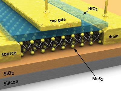
The discovery made in the EFPL can play an important role in the field of electronics, which will make it possible to create more energy efficient transistors of a much smaller size than now. Research has shown that molybdenite (or MoS2) is a very efficient semiconductor. This mineral, which exists in abundance in nature, is often used as an element of steel alloys or as an additive in lubricants. But so far has not been investigated for use in electronics.
“This is a two-dimensional material, very thin and easy to use in relation to the field of nanotechnology. He has real potential in the field of manufacturing very small transistors, light-emitting diodes (LEDs) and solar batteries, ”said EFPL professor Andras Kees, who, not without the help of his laboratory colleagues, did a great job and carried out this research. He compares the advantages of molybdenite with silicon, which is currently the main component used in the production of electronic and computer chips, and graphene, opened in 2004 by two physicists of the University of Manchester - Andre Geim and Konstantin Novoselov, for which they were awarded the Nobel Prize in Physics 2010
One of the advantages of molybdenite is that it is less voluminous than silicon, which is a three-dimensional material. In a 0.65 nanometer-thick molybdenite sheet, electrons can move as easily as in a two-nanometer-thick silicon sheet, ”explains Kies. "At the same time, it is not possible to manufacture a sheet of silicon as thick as a monolayer of molybdenite today."
Another advantage of the new material is the ability to manufacture transistors that consume 100,000 times less energy in standby mode than traditional silicon transistors. The presence of a “forbidden zone” (gap) 1.8 eV wide in molybdenite makes it an almost ideal semiconductor.
')
The band theory in solid state physics is a quantum-mechanical theory of the motion of electrons in various materials. In semiconductors, spaces free of electrons are called "forbidden zones". If this zone is not too small or too large, some electrons can pass through it. Thus, a higher level of control over the electrical behavior of the material is possible.
The existence of a “forbidden zone” in molybdenite gives it an advantage over graphene. This “semimetal”, currently considered by many scientists as the material of the future, does not have such zones, and it is very difficult to reproduce them artificially.
Via eurekalert
Source: https://habr.com/ru/post/112890/
All Articles