220V device control via LPT port (full creation cycle)
Prehistory
After reading the article on Habré about controlling the lamp via the Internet, I had an idea to control the lighting at home from a computer, and since I’ve already set up controlling a computer from a cell phone, this means that the light can be controlled from the same phone. After demonstrating the article to one of my colleagues, he said that he needed it. Since he often watches films that he watches on a computer, he falls asleep. The computer some time after the end of the film also falls asleep and turns off the monitor, but the light in the room remains on. Those. it was decided that the thing was useful, and I began to collect information and details for this miracle.
The rest of the information under the habracut (cautiously a lot of pictures - traffic).
Device layout
For the original scheme was taken one of the schemes found on the Internet and it looked like this:

But only with a slight change: a resistor of 390 ohms was added between the first pin of the 4N25 optocoupler and the second pin of the LPT, and another LED was added to indicate switching on. The scheme was assembled in test mode, i.e. just wired as needed and tested. In this version, she simply turned on and off the old Soviet torch.
It was decided that if you already had control, it was not for one device, but for at least 4 devices (at the rate of: one lamp on the table, a chandelier for two switches, a spare socket). At this stage, it became necessary to build a complete scheme of the device, the choice of various programs began.
Were installed:
- Pbc
- Kicad
- gEDA
- Eagle
After looking at all of them, I stopped at Eagle, as there were “similar” details in its library. That's what happened in it:

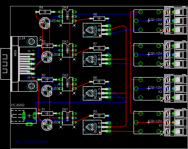
The diagram used port DB9 ie An ordinary COM port, this is done for reasons of economy, both on board and on the connectors themselves (I had COMs), and since we will only use 5 conductors, this is enough for us with a margin. So we also do the adapter from DB25 (LPT) to DB9 (COM), in my case it is done as follows:
LPT 2-9 pin = COM 1-8 pin - these are control data pins;
LPT 18-25 pin (they are often interconnected) = COM 9 pin - this is our land.
Also, the circuit uses additional 12V power supply to power the relay, according to the plan it will be a simple Chinese charger or maybe 9V crown (one relay works normally, you need to check for 4 at a time). Separate power and galvanic isolation using optocouplers is used to secure the computer port. If you wish, you can of course be powered from a 12V power supply unit of a computer, but this each does on its own and at its own peril and risk.
')
Necessary parts to create a device
- COM port - 1 pc
- power connector - 1 pc
- green LED - 4 pcs
- optocoupler 4n25 - 4 pieces
- seat for optocoupler (I only had 8 feet) - 4 pcs
- 390 ohm resistor - 4 pcs
- 4.7 kΩ resistor - 4 pcs
- KT815G transistor - 4 pieces
- Relay HJR-3FF-SZ - 4 pcs
- clips on 3 contacts - 4 pieces
- foil textolite
Preparing the circuit board
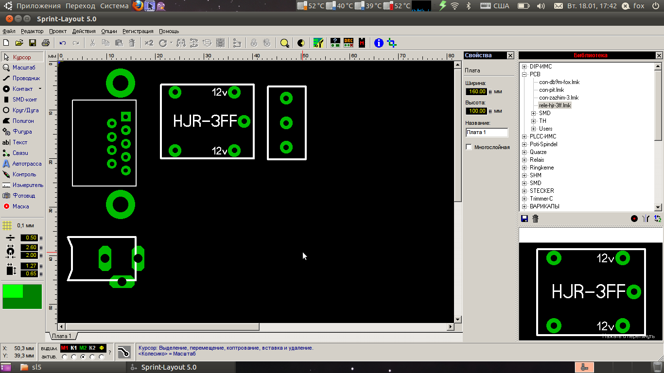
Having tried to use Eagle for preparing the printed circuit board, I realized that it would be difficult and decided to find a simpler version. This option was the sprint layout 5 program, even if it is for windows, but runs without problems in wine under linux. The interface of the program is intuitive, in Russian and in the program there is quite clear help (help). Therefore, all further actions for the development of the printed circuit board were made in sprint layout 5 (hereinafter referred to as SL5).
Although many people use this program to develop the boards of their devices, I didn’t have the details I needed (even in a heap of downloaded macro collections). Therefore, we had to first create the missing parts:
- COM port (the one that did not coincide with mine, through the mounting holes)
- power socket
- three contact clip
- relay HJR-3FF-SZ
View of these details:
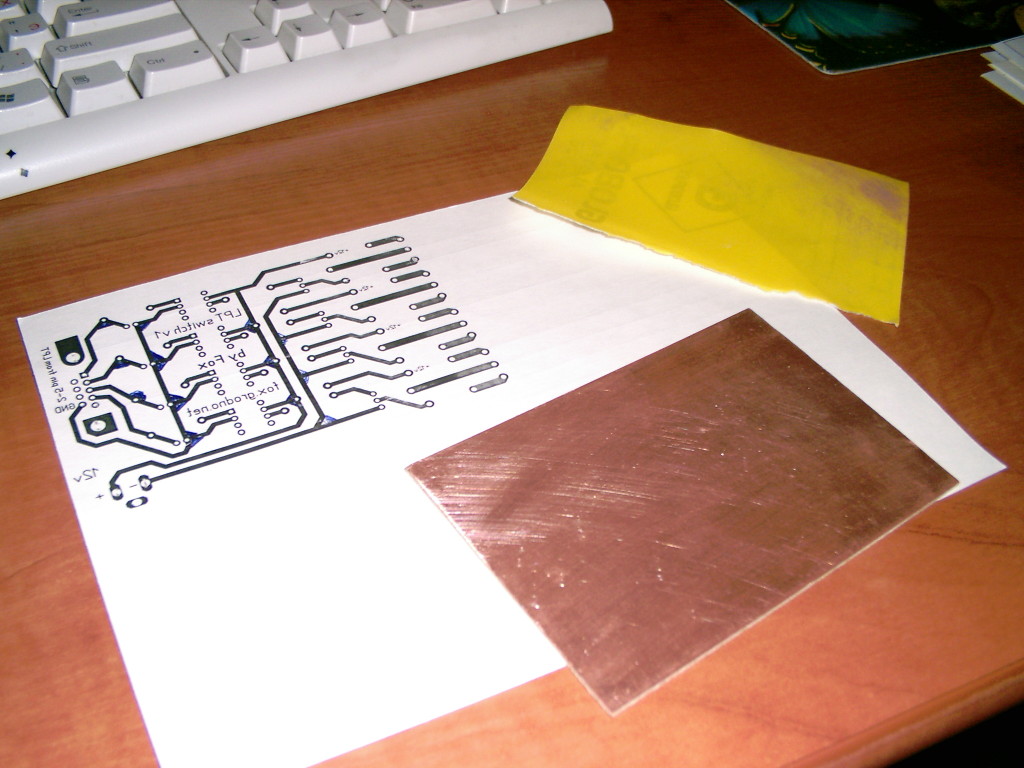
After adding the necessary details, the design of the PCB itself began. It passed in several attempts, there were about five of them. Each version of the board was printed on cardboard, holes were punctured and parts were inserted into them. Actually, it was found out that my COM port does not match the one that was in SL5. Just a small error surfaced in the relay circuit - in fact, the relay body was shifted by 2-3 mm. Naturally all the errors have been corrected.
On the first printed version, it turned out that the transistor connection was not correct, two contacts were mixed up.
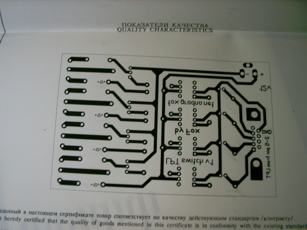
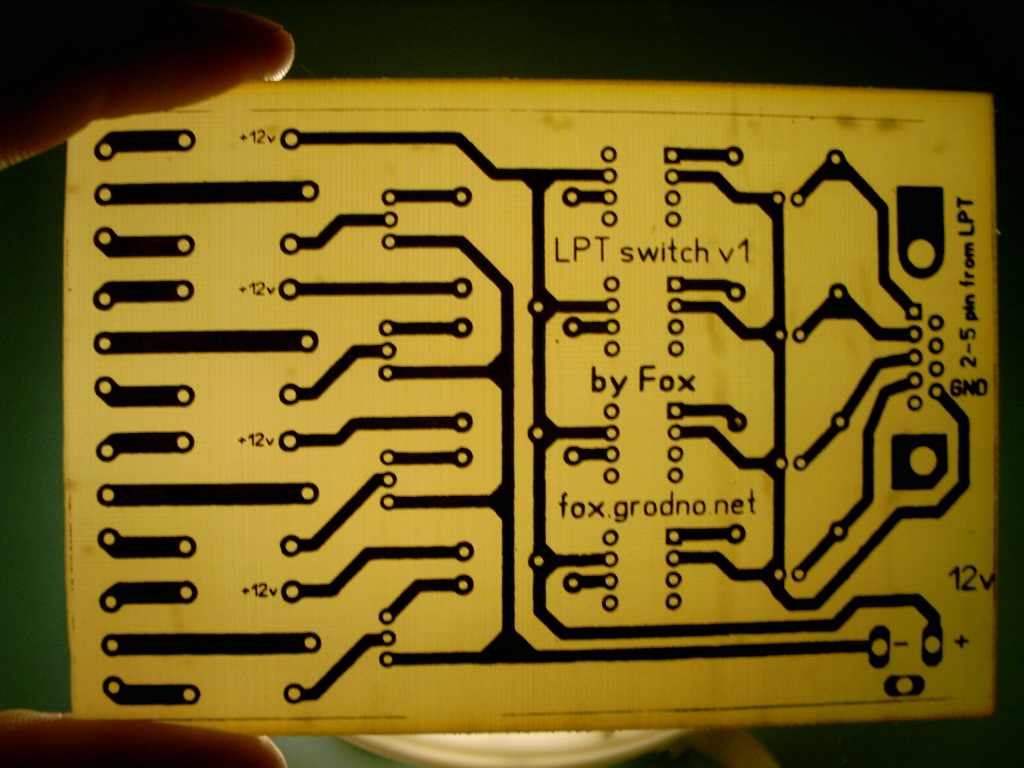
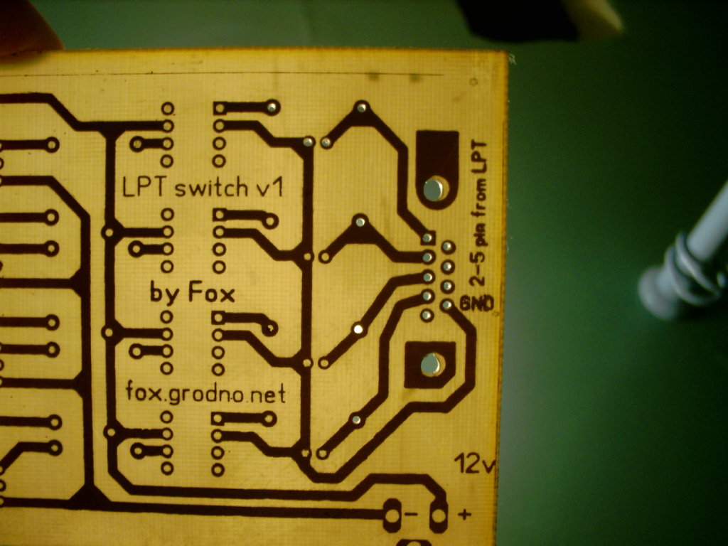
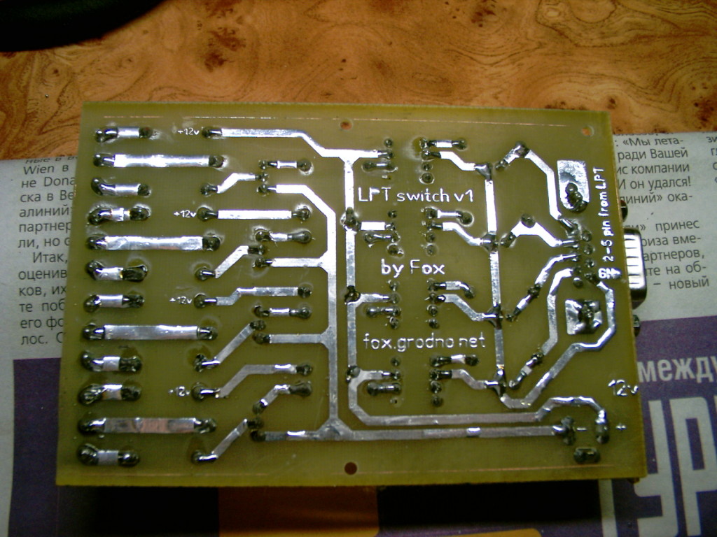
After all the corrections and fits, it turned out to be the following board:
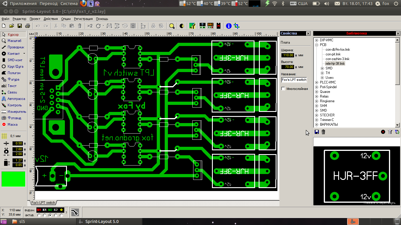
In SL5 there is a “Photo View” function for viewing the board, here’s how it looks in it:
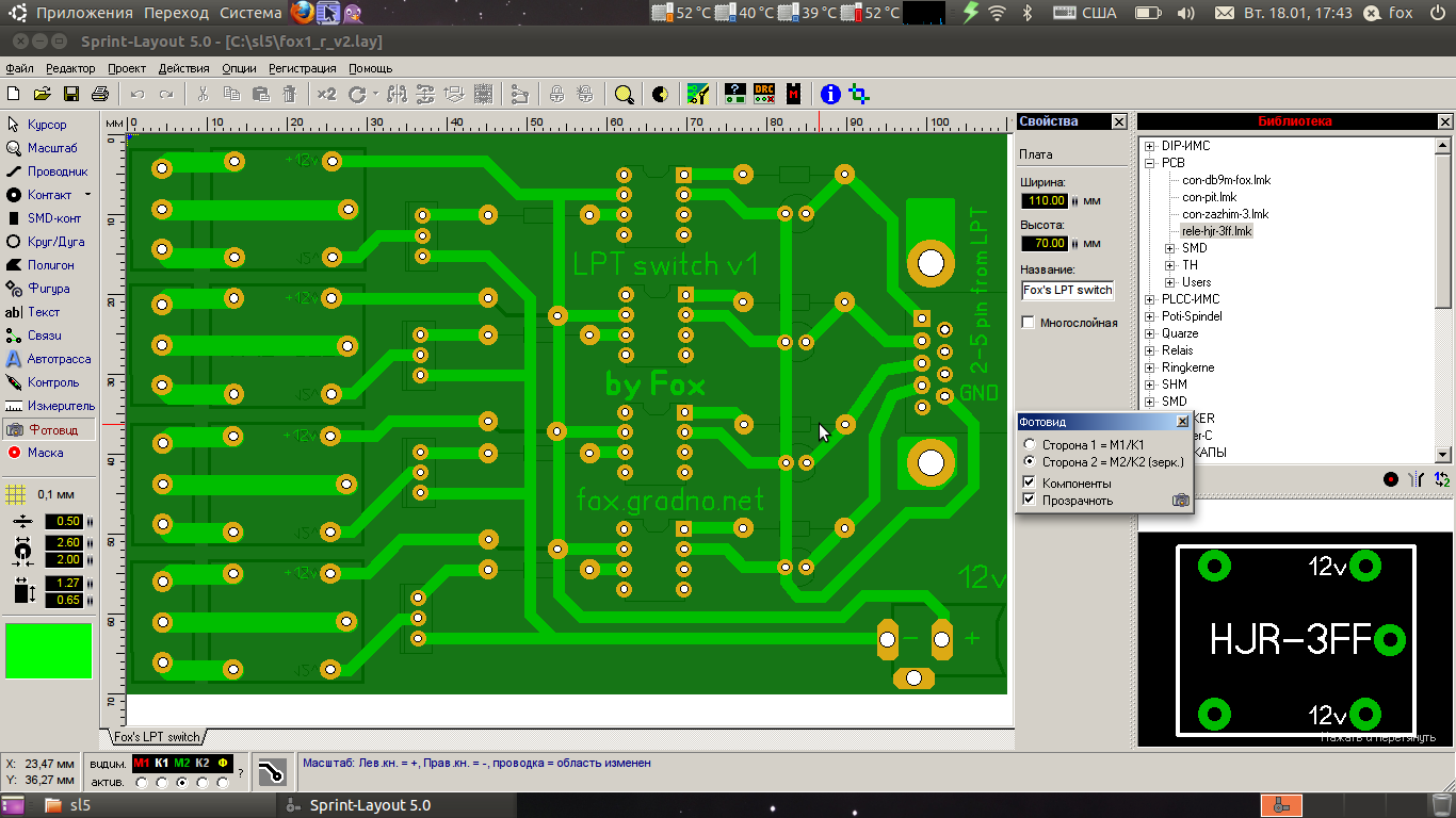

In the final version of the board, the tracks will be slightly corrected, but otherwise it looks the same.
In SL5 there is also a convenient option for printing the board, you can hide unnecessary layers and choose the print color of each layer, which is very useful.
PCB preparation
It was decided to make the board using the LUT method (laser-iron technology). Next, the whole process in the photo.
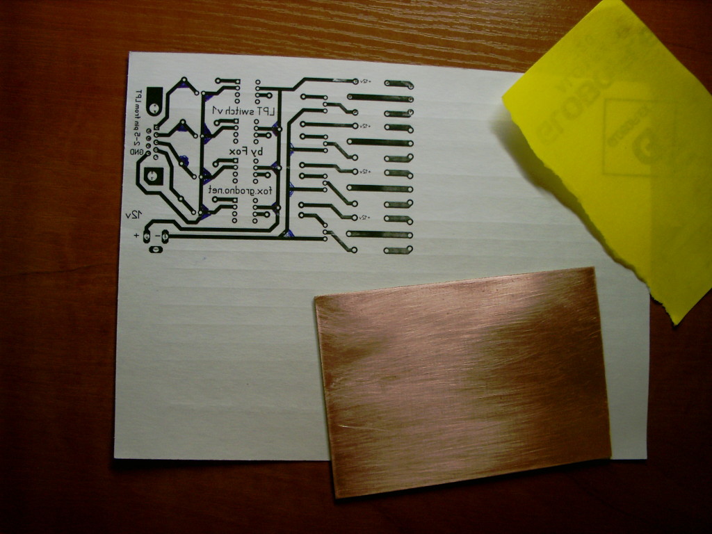
Cut out the required size of a piece of textolite.
We take the smallest sandpaper and gently we clean the copper surface.
After stripping the surface, it must be rinsed and degreased. You can rinse with water, and degrease with acetone (in my case it was solvent 646).
Then we print our board on a laser printer on coated paper, without forgetting to install the most bold print in the printer (without saving toner). This option turned out a bit unsuccessful, since the toner was smeared, but another attempt was just right.
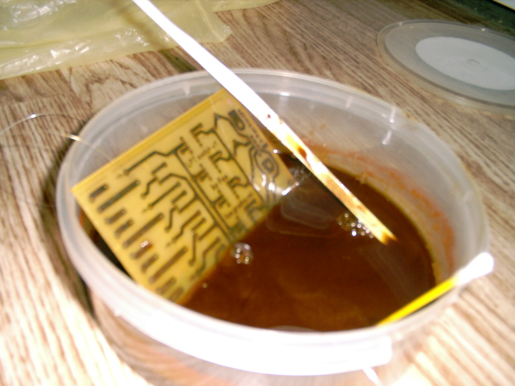
Now you need to transfer the picture from paper to textolite. To do this, we cut out the picture and apply it to the PCB, we try to align it as needed and then heat it with an iron. It is necessary to thoroughly heat the entire surface so that the toner melts and sticks to the copper surface. Then we give the board to cool down a bit and go to wet it under running water. When the paper is well enough wet it must be separated from the board. Only adhered toner will remain on the board. It looks like this:

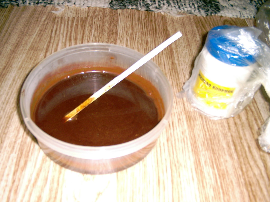
Next, you need to prepare a solution for etching. I used ferric chloride for this. It is written on the ferric chloride bank that the solution needs to be done 1 to 3. I stepped back a bit from this and made 60 g of ferric chloride per 240 g of water, i.e. it turned out 1 to 4, in spite of this board etching was normal, only a little slower. Pay attention that the process of dissolving dry ferric chloride in water proceeds with the evolution of heat, therefore it is necessary to pour it into the water in small portions and stir it. Naturally, it is necessary to use non-metallic dishes for pickling, in my case it was a plastic container (sort of from herring). I got this solution:
Before lowering the board into the solution, I glued a line to the back of the line with the help of an adhesive tape, which would be more convenient to get the board and turn it over. If the solution gets on your hands, you must quickly wash it off with soap (the soap neutralizes it), but the stains may still remain, it all depends on the specific conditions. Stains from clothes are not displayed at all, but I was lucky not to check this for myself. Immersing the board into the solution should be copper down and not all flat, but at an angle. From time to time it is advisable to clear the board from working off, as it prevents further etching. This can be done with cotton swabs.

The whole etching process took me 45 minutes, 40 minutes would be enough, but I was just busy with one more thing.
After etching, wash the board with soap and tear off the tape with the line and get:
Attention! Do not pour the solution of ferric chloride into the sink (sewage) - this may damage the metal parts of the sink, and in general the solution may still be useful.
Next, we need to wash off the toner, this is successfully done with the same solvent 646 that was used for degreasing (long contact of the solvent with the skin can damage it).

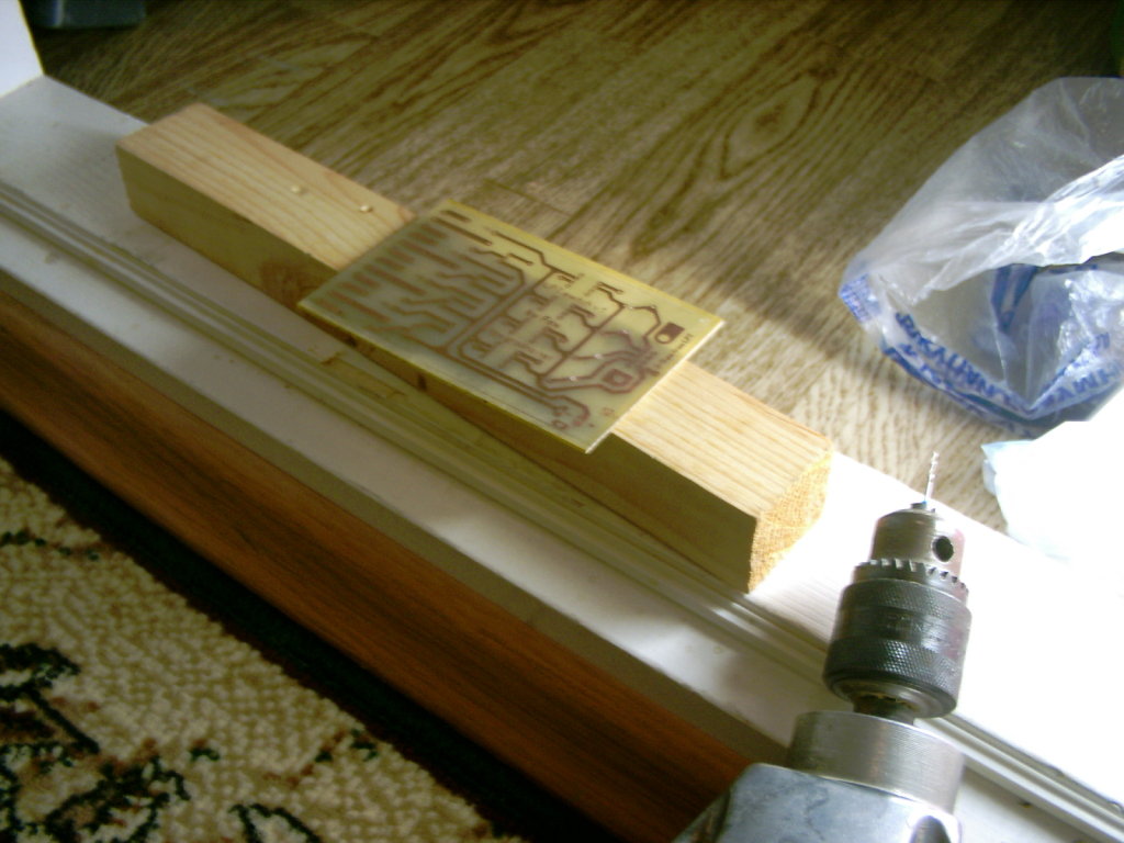
The next step is to drill holes. I had 1mm and 1.5mm holes on the board, initially, since it was not possible to find thinner drills. It was also impossible to find a collet chuck for mounting it on an electric motor in our city, so everything was done with a big drill.
The first device came up

The first time I took only two drills, but when using such a drill this turned out to be not enough. One drill broke, and the second bent. All that I managed to drill on the first day:
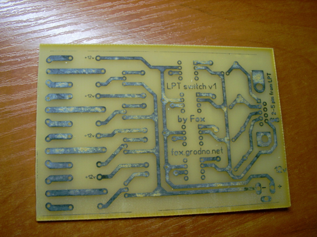
The next day I bought five drills. And they were just enough, because if they do not break (by the way, only one broke out of the five), they become blunt, and when bored, the tracks deteriorate, the copper begins to flake off. After complete drilling of the board we get:


After drilling it is necessary to conduct a tin plating. For this, I used the old method - a soldering iron, a TAGS flux and tin. I wanted to try using the Rosa alloy, but not to find it in our town.
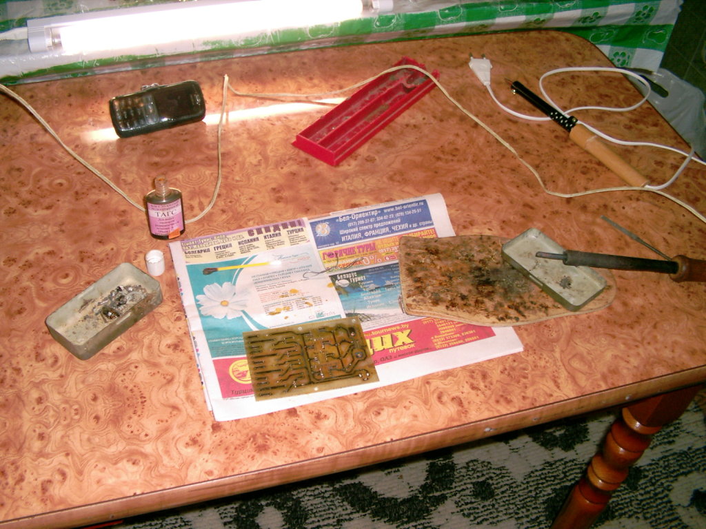
After tinning we get the following result:


Next, you need to wash the board to remove residual flux, since the TAGS is water-washed, this can be done either with water or with alcohol. I did something mean - laundered old vodka and rubbed with cotton buds. After all these actions, our board is ready.
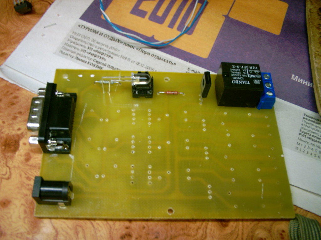
Mounting parts
To verify the correctness of the board, I initially collect only one (out of four) line of parts, where the error has crept in.
After mounting the parts, go and connect the device to the computer via LPT, for this an adapter is connected from DB25 (LPT) to DB9 (COM) in the following form:
- 2 pin DB25 to 1 pin DB9
- 3 pin DB25 to 2 pin DB9
- 4 pin DB25 to 3 pin DB9
- 5 pin DB25 to 4 pin DB9
- 6 pin DB25 to 5 pin DB9
- 7 pin DB25 to 6 pin DB9
- 8 pin DB25 to 7 pin DB9
- 21 pin DB25 (can be any from 18 to 25) to 9 pin DB9
Since ordinary twisted pair was used as a wire, one wiring was not enough, but only five wires are enough for this device, so this option is suitable. As an included load we have a simple Soviet flashlight. Well, as a power supply - universal Chinese power supply (4 connectors and power from 3 to 12). Here are all in the collection:

But the device is already working:
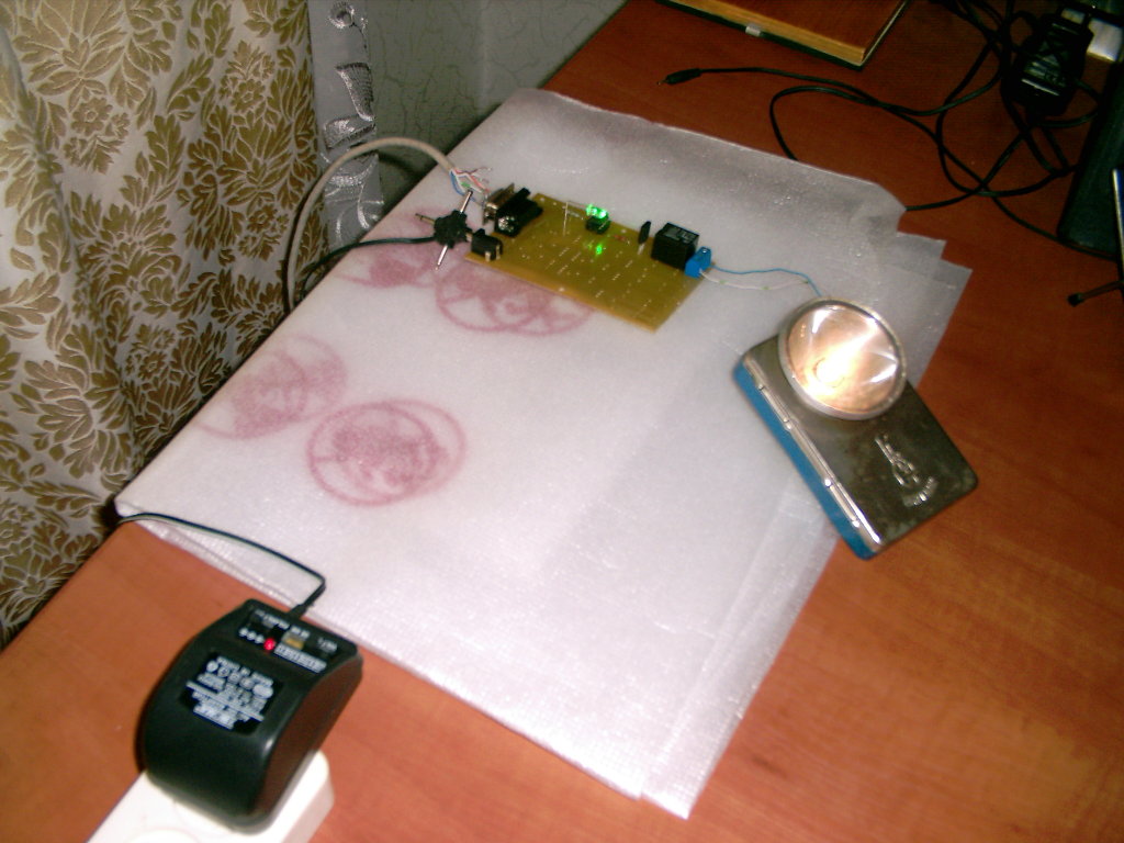
This ended another evening and the installation of the remaining parts was left the next day.
And here is the fully assembled device:

Well, a little video about how it works (the quality is not very good, there was nothing to take off normally)
That's all, it remains only to find a normal case for the device and run it in the case.
Software part
Naturally, to manage the LPT port, you need some kind of software, but since I have linux at my home, it was decided to simply write the simplest program myself, and later it would need to be added and adapted as necessary. She looked like this:
#include <stdio.h>
#include <stdlib.h>
#include <unistd.h>
#include <sys/io.h>
#define BASE 0x378
#define TIME 100000
int main ()
{
int x = 0x0F;
int y = 0x00;
if (ioperm (BASE, 1, 1))
{
perror ("ioperm()");
exit (77);
}
outb (x, BASE);
return 0;
}
This program sends to LPT port 0x0F = 00001111, i.e. delivers 1 to 2-5 pins (Data0-Data3), and this is our control voltage between 2-5 pins and ground (18-25 pins), thus all four relays will be turned on. Similarly, there is a program for sending 0x00 to the port for disconnecting, instead of x, just sending y - outb (y, BASE). You can also read the port status:
#define BASEPORT 0x378 /* lp1 */
...
printf(": %d\n", inb(BASEPORT));
...
The only nuance of this program is that it needs to be performed as root, since the ioperm function is not available to the simple user. I think how to solve such a problem can not tell, everyone will choose a more suitable option.
Subsequently, the program was refined so that passing the command line parameters to it could indicate with which device and what to do.
The “sw --help” output:
LPT .
.
: sw [ ] []
- 1 8
- "on", "off", "st" - , ,
: "sw 2 on" "sw --help"
PS If someone needs it, then I can somewhere lay out the circuit card file in sl5 and the source code of the control program.
Source: https://habr.com/ru/post/112511/
All Articles