Development of digital devices based on VLSI programmable logic
On Habré periodically appear articles on the development of equipment. However, most of them proceed from theoretical positions (what are logical elements, triggers, etc.) and stop at this, or consider the issue in the aspect of “do it yourself”, i.e. what a person can create on their own at home. I would like to talk about how the hardware design procedure looks from the point of view of a small company earning it with bread and butter.
But first, a few words about the specifics of this area (at least in our country). It is necessary to proceed from the following realities:
One of the few successful models is contract development for Western customers. The idea is simple: high-tech research / development is ordered from us, the results are gathered together somewhere in California (usually along a chain through several intermediaries) and end up being sold to some large electronics manufacturing corporation. The same Intel, for example. After 2-3 years, all this comes back to us as part of complex units (telephones, monitors, etc.) in a beautiful box with the “Made in USA” stamp (which is rare) or “Made in China” (much more often) by gold pieces for the bundle. On the one hand, the situation is sad - we do not own the technological chain, but are able to solve only individual tasks. But there is also reason for optimism - in this way, Russian developers enter the global system and gain valuable experience. The company in which I work, specializes mainly in research developments in the field of wireless communications. Based on this, I will lead a further story.
What does the development process look like?
Initially, the customer provides some information (suggestions) on what tasks need to be solved and in what form to present the result. Usually, these are mathematical models that implement the algorithms that are to be developed and the equipment, with the help of which one can demonstrate the embodiment of the algorithms "in hardware". When both parties interact, a technical assignment (TOR) is drawn up, which contains complete information about the parameters of the device being created (frequency ranges, data rates, used modulation types, etc.), requirements for device characteristics and testing methods. As you might guess (miracles, alas, does not happen), in the development process, these parameters can be adjusted (both on the one hand and on the other) and you have to look for compromises. In general, the structure of the device being created (phone, modem) for wireless data transmission looks like this:

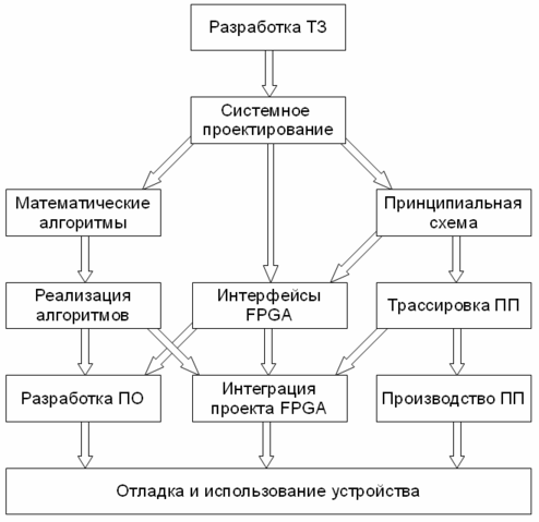
The next step is a system design . Draws a block diagram of the device and communication between components. An assessment of the resource intensity of the task is made, the equipment that will implement the algorithms being created is selected. By and large, there are three ways:
The parameters of other critical elements of the system being created are also recorded - the necessary frequencies of the ADC and DAC, the RF parameters (radio path - the high-frequency part) and others.
')
The subsequent stages pass in parallel as the previous ones are ready. Initially, the development of mathematical algorithms and the development of the electrical circuitry of the device are launched.
The development of mathematical algorithms usually begins with the study of thematic literature and drawing some basic things on a piece of paper. However, the theoretical approach, unfortunately, is weakly applied due to the great complexity of the algorithms being created. In this regard, rather quickly, the design process proceeds to the use of a special CAD system for simulation modeling. It allows you to create models by “drawing” them in graphical mode from the basic library blocks and the connections between them. These library blocks can be objects of completely different complexity - from adders and logic gates to finished filters, modulators, etc.
In addition to the model of the device itself, a test environment is also created - the components that generate test signals (the same as in real life) and the components responsible for assessing the quality of the device operation. If we talk about the telecommunications area, then, depending on the specific type of device being created, they usually operate with such basic characteristics as SNR (signal-to-noise ratio) and BER (bit error rate) error occurrence in the channel).
The procedure of creating a mathematical model is iterative - the first version of the model is created, tests are run, the resulting characteristics are evaluated. Then something is corrected / supplemented, tests are run again and so on until the requirements of the TOR are met.
Traditionally used for these tasks, CAD - Matlab / Simulink and SPW. The first of them has received much more widespread (at least in our country).
After creating mathematical models, it becomes possible to implement algorithms on FPGA . Depending on the requirements of the customer, different approaches can be applied, but the main trend is the maximum automation of the stage (as indeed in many other places) based on the existing mat. models. Design tools are actively developing these capabilities. In the event that mat. the model is made using a number of special rules, it can be automatically adapted to a form suitable for use in an FPGA project. From the point of view of the developer, everything looks (in an ideal situation) very simply - I pressed the button and got the VHDL / Verilog code corresponding to the original model. Unfortunately, there are 2 problems that make this approach difficult:
One way or another, eventually mat. the model is presented in the form of code that can be integrated into the main FPGA project.
In the development of electrical concepts in the first place is the choice of electronic components based on their characteristics, as well as accessibility (for purchase). In Russia, the delivery time for components (except for those already located in Russian distributors' warehouses) is very high and customers can help in purchasing components (provided that they are located in Europe / USA / Southeast Asia and not somewhere in Africa). But even in this case, there are situations that the delivery time of the necessary components can be 20-30 weeks and then you have to look for a replacement (and, sometimes, make changes to the fee already divorced).
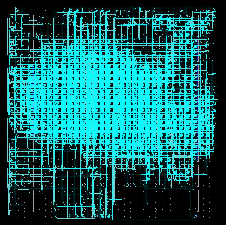
Upon completion of the creation of the electrical circuit, the next, closely related stage starts: tracing the printed circuit board . All selected components of the device are placed on a printed circuit board (PCB) and connections are created between them in accordance with the scheme. Depending on the complexity (board dimensions, installation density of components and their number), the number of layers of the printed circuit board is usually 4-12. Naturally, they try to minimize their number, but ultimately it all depends on the requests of the person who is engaged in tracing (the rapper) and his experience. The tracing process takes into account many requirements regarding the integrity and propagation time of signals over an AC.
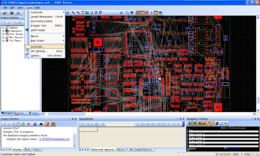
Design tools such as Pads (Expedition) from Mentor Graphics, Cadence OrCAD (Allegro) and Altium Designer are most commonly used to design the layout and tracing. In the Russian outback, they continue to actively use P-CAD (and not the latest version), but if you offer a scheme implemented in this way to a western customer, they will not understand you (the release of new versions of P-CAD was completed 5 years ago, support was discontinued in 2008).
After creating the final (he-he) version of the PP trace, it is put into production, all subsequent modifications are made with a scalpel, a soldering station and a wire. The board itself is made most often in the Southeast Asian region (usually through Russian intermediaries), the components are soldered in Russia (as close as possible so that it is not far to bring the soldering problems to correct). In view of the small circulation and high complexity of the boards created (we agreed in the introduction), the process is not perfect and therefore every board is manually debugged / repaired during commissioning.
After the device layout is ready (that is, the list of components with which the FPGA will communicate) is known, you can begin developing the interface-service functions of the FPGA . Development of the project for FPGA is made using special design languages. The de facto standards at the moment are VHDL and Verilog. Syntactically, the first of them is similar to Hell (Pascal), the second to Xi. However, these languages have a fundamental difference - they are not intended to describe sequential programs (although they can also be used for these purposes too), but to describe hardware, i.e. parallel structures. The most common way to describe the equipment is the name RTL (register transfer level). At the same time, memory objects (triggers, registers, memory blocks) and rules for transferring (and transforming) data between them (logic, combination schemes) are described. Not to be unfounded, the description of the simplest counter on VHDL looks like this:
In the future, DSP-algorithms are integrated into the same model and the last changes are made upon completion of the PCB trace phase ( integration of the FPGA project ). By and large, all that was said above about the creation of a project based on FPGA is also true when designing an ASIC, only the level of responsibility is much higher, since there is no chance to correct the error. After the project is created, it is compiled (automatically using various CAD systems, depending on the type of FPGA used) and the project is ready for programming into a chip. If the production plan is made without gross miscalculations, then approximately by this time the board comes from the production and begins its testing, and further operation (demonstration of the work of the created algorithms). Naturally, in the course of work, these algorithms can be changed and supplemented, and the “reprogrammable” FPGA allows you to quickly bring them into the project.
Another important design stage is the development of the software part of the project . The software being created is divided into two categories: implementation of the user interface on a PC (if manual device control or data exchange is required) and firmware creation (if it is necessary to implement complex control algorithms directly on the device that are inconvenient to create with logic - in this case or on the board a separate control processor, or a software core of the processor is used, embedded in the FPGA).
After the printed circuit board is received and soldered, a project for the FPGA is created and software capable of managing it is developed, the testing and debugging process begins. But that's another story.
But first, a few words about the specifics of this area (at least in our country). It is necessary to proceed from the following realities:
- it is impossible in our conditions to compete with Intel or at least TI in the release of processors and other different microcircuits - the price of entry is very high, the sales markets are divided, and, by and large, there is no necessary knowledge and experience;
- it makes no sense to compete with the Chinese in the production of all kinds of mass electronics - their labor costs are lower, their production facilities are in the hands of large companies;
- You can spud domestic markets with a variety of uncomplicated electronics - from alarms to Christmas tree garlands. Someone lives this, but the rate of profit is low, and there is a lot of trouble;
- You can participate in the state program to support the poor (RosPil). Great theme, but forgot to invite me.
One of the few successful models is contract development for Western customers. The idea is simple: high-tech research / development is ordered from us, the results are gathered together somewhere in California (usually along a chain through several intermediaries) and end up being sold to some large electronics manufacturing corporation. The same Intel, for example. After 2-3 years, all this comes back to us as part of complex units (telephones, monitors, etc.) in a beautiful box with the “Made in USA” stamp (which is rare) or “Made in China” (much more often) by gold pieces for the bundle. On the one hand, the situation is sad - we do not own the technological chain, but are able to solve only individual tasks. But there is also reason for optimism - in this way, Russian developers enter the global system and gain valuable experience. The company in which I work, specializes mainly in research developments in the field of wireless communications. Based on this, I will lead a further story.
What does the development process look like?
Initially, the customer provides some information (suggestions) on what tasks need to be solved and in what form to present the result. Usually, these are mathematical models that implement the algorithms that are to be developed and the equipment, with the help of which one can demonstrate the embodiment of the algorithms "in hardware". When both parties interact, a technical assignment (TOR) is drawn up, which contains complete information about the parameters of the device being created (frequency ranges, data rates, used modulation types, etc.), requirements for device characteristics and testing methods. As you might guess (miracles, alas, does not happen), in the development process, these parameters can be adjusted (both on the one hand and on the other) and you have to look for compromises. In general, the structure of the device being created (phone, modem) for wireless data transmission looks like this:
The next step is a system design . Draws a block diagram of the device and communication between components. An assessment of the resource intensity of the task is made, the equipment that will implement the algorithms being created is selected. By and large, there are three ways:
- Use DSP processors (digital signal processors). They are good in situations where it is necessary to implement complex algorithms for data flow following at a not very high speed - algorithms that are conveniently described using sequential programs. Unfortunately, their performance is not enough in all cases. Several billion multiplications per second is not much at data stream rates of the order of 100 MHz or more.
- Customized VLSI (ASIC) - a great way for the rich and courageous. They are designed for a specific task, and therefore do not contain unnecessary logic; working frequencies 1-2 GHz. In cases where it is planned to produce a large batch of devices (hundreds of thousands of pieces), the creation of customized VLSI allows you to get the maximum performance at the lowest price per item. Unfortunately, the pleasure is very expensive. Creating one revision of microcircuits for not the most modern technological standards costs about 1 million dollars.
- VLSI Programmable Logic (FPGA) is a compromise for those who create prototype devices (circulation - a few pieces). They contain many standard blocks that perform certain tasks. The user is given the opportunity to customize the parameters of these blocks and establish links between them. Modern FPGAs are capable of operating at frequencies up to 500 MHz and at the same time contain up to 1000 built-in hardware multiplication units (plus logic elements, built-in memory, high-speed transceivers, etc.). Pleasure is also not cheap - one chip of this class will cost 10-15 thousand dollars. Naturally, such a large crystal is not always required. In my practice, the cost of used FPGA is usually $ 300-2000 (if we talk about DSP tasks). The two main FPGA manufacturers, Xilinx and Altera, collectively occupy more than 80% of the programmable logic market. The rulers of the chips of both companies have similar parameters and, often, the choice between them is not due to technical characteristics, but to the preferences of the customer.
The parameters of other critical elements of the system being created are also recorded - the necessary frequencies of the ADC and DAC, the RF parameters (radio path - the high-frequency part) and others.
')
The subsequent stages pass in parallel as the previous ones are ready. Initially, the development of mathematical algorithms and the development of the electrical circuitry of the device are launched.
The development of mathematical algorithms usually begins with the study of thematic literature and drawing some basic things on a piece of paper. However, the theoretical approach, unfortunately, is weakly applied due to the great complexity of the algorithms being created. In this regard, rather quickly, the design process proceeds to the use of a special CAD system for simulation modeling. It allows you to create models by “drawing” them in graphical mode from the basic library blocks and the connections between them. These library blocks can be objects of completely different complexity - from adders and logic gates to finished filters, modulators, etc.
In addition to the model of the device itself, a test environment is also created - the components that generate test signals (the same as in real life) and the components responsible for assessing the quality of the device operation. If we talk about the telecommunications area, then, depending on the specific type of device being created, they usually operate with such basic characteristics as SNR (signal-to-noise ratio) and BER (bit error rate) error occurrence in the channel).
The procedure of creating a mathematical model is iterative - the first version of the model is created, tests are run, the resulting characteristics are evaluated. Then something is corrected / supplemented, tests are run again and so on until the requirements of the TOR are met.
Traditionally used for these tasks, CAD - Matlab / Simulink and SPW. The first of them has received much more widespread (at least in our country).
After creating mathematical models, it becomes possible to implement algorithms on FPGA . Depending on the requirements of the customer, different approaches can be applied, but the main trend is the maximum automation of the stage (as indeed in many other places) based on the existing mat. models. Design tools are actively developing these capabilities. In the event that mat. the model is made using a number of special rules, it can be automatically adapted to a form suitable for use in an FPGA project. From the point of view of the developer, everything looks (in an ideal situation) very simply - I pressed the button and got the VHDL / Verilog code corresponding to the original model. Unfortunately, there are 2 problems that make this approach difficult:
- Mat. A model is usually created for floating-point numbers, while inside FPGA calculations are traditionally performed in a fixed-point format (this is much faster and less resource-intensive). In this regard, it is necessary to create an intermediate model, made in a fixed-point format. This stage is performed manually, although now there is an active development of the means to automate this stage.
- Mat. the model is created without additional delays, which are necessary in the equipment for the successful operation of the device at the required frequencies (so-called pipelining). In addition, the introduction of such delays in feedback algorithms affects the stability of the system and requires careful re-modeling.
One way or another, eventually mat. the model is presented in the form of code that can be integrated into the main FPGA project.
In the development of electrical concepts in the first place is the choice of electronic components based on their characteristics, as well as accessibility (for purchase). In Russia, the delivery time for components (except for those already located in Russian distributors' warehouses) is very high and customers can help in purchasing components (provided that they are located in Europe / USA / Southeast Asia and not somewhere in Africa). But even in this case, there are situations that the delivery time of the necessary components can be 20-30 weeks and then you have to look for a replacement (and, sometimes, make changes to the fee already divorced).
Upon completion of the creation of the electrical circuit, the next, closely related stage starts: tracing the printed circuit board . All selected components of the device are placed on a printed circuit board (PCB) and connections are created between them in accordance with the scheme. Depending on the complexity (board dimensions, installation density of components and their number), the number of layers of the printed circuit board is usually 4-12. Naturally, they try to minimize their number, but ultimately it all depends on the requests of the person who is engaged in tracing (the rapper) and his experience. The tracing process takes into account many requirements regarding the integrity and propagation time of signals over an AC.
Design tools such as Pads (Expedition) from Mentor Graphics, Cadence OrCAD (Allegro) and Altium Designer are most commonly used to design the layout and tracing. In the Russian outback, they continue to actively use P-CAD (and not the latest version), but if you offer a scheme implemented in this way to a western customer, they will not understand you (the release of new versions of P-CAD was completed 5 years ago, support was discontinued in 2008).
After creating the final (he-he) version of the PP trace, it is put into production, all subsequent modifications are made with a scalpel, a soldering station and a wire. The board itself is made most often in the Southeast Asian region (usually through Russian intermediaries), the components are soldered in Russia (as close as possible so that it is not far to bring the soldering problems to correct). In view of the small circulation and high complexity of the boards created (we agreed in the introduction), the process is not perfect and therefore every board is manually debugged / repaired during commissioning.
After the device layout is ready (that is, the list of components with which the FPGA will communicate) is known, you can begin developing the interface-service functions of the FPGA . Development of the project for FPGA is made using special design languages. The de facto standards at the moment are VHDL and Verilog. Syntactically, the first of them is similar to Hell (Pascal), the second to Xi. However, these languages have a fundamental difference - they are not intended to describe sequential programs (although they can also be used for these purposes too), but to describe hardware, i.e. parallel structures. The most common way to describe the equipment is the name RTL (register transfer level). At the same time, memory objects (triggers, registers, memory blocks) and rules for transferring (and transforming) data between them (logic, combination schemes) are described. Not to be unfounded, the description of the simplest counter on VHDL looks like this:
process(clk, rst)
begin
if rst = '1' then cnt <= 0;
elsif rising_edge(clk) then
cnt <= cnt + 1;
end if;
end process;
Naturally, it is possible to build hierarchical descriptions using components developed by both you and third-party developers. Another way to describe a project for FPGA is through graphical input. In this case, using a special editor, you compose your devices from various components and connect them together. There are endless religious wars on this topic, a brief summary of which — the description of the algorithmic part in a schematic way — is evil, since the project is not being followed up (only the author can understand it for a short time); the description of the upper levels of the hierarchy in a graphical way can be convenient (allows a person to evaluate the structure of the system as a whole), but makes it difficult to work with such files of automatic text file comparison tools (search for changes). For debugging of created components, tests are written, most often on the same VHDL / Verilog, which allow you to verify in the automatic or manual (I analyze time diagrams) mode that the unit is working correctly.In the future, DSP-algorithms are integrated into the same model and the last changes are made upon completion of the PCB trace phase ( integration of the FPGA project ). By and large, all that was said above about the creation of a project based on FPGA is also true when designing an ASIC, only the level of responsibility is much higher, since there is no chance to correct the error. After the project is created, it is compiled (automatically using various CAD systems, depending on the type of FPGA used) and the project is ready for programming into a chip. If the production plan is made without gross miscalculations, then approximately by this time the board comes from the production and begins its testing, and further operation (demonstration of the work of the created algorithms). Naturally, in the course of work, these algorithms can be changed and supplemented, and the “reprogrammable” FPGA allows you to quickly bring them into the project.
Another important design stage is the development of the software part of the project . The software being created is divided into two categories: implementation of the user interface on a PC (if manual device control or data exchange is required) and firmware creation (if it is necessary to implement complex control algorithms directly on the device that are inconvenient to create with logic - in this case or on the board a separate control processor, or a software core of the processor is used, embedded in the FPGA).
After the printed circuit board is received and soldered, a project for the FPGA is created and software capable of managing it is developed, the testing and debugging process begins. But that's another story.
Source: https://habr.com/ru/post/111544/
All Articles