From sand to processor
It is difficult to believe in it, but a modern processor is the most complex finished product on Earth - and in fact, it would seem, why is it difficult in this piece of iron?
As promised - a detailed account of how processors are made ... starting with the sand. Everything you wanted to know, but were afraid to ask)
')
I have already talked about " Where do the processors produce " and about what " Production Difficulties " stand in this way. Today we will speak directly about the production itself - “from and to”.
When a factory for manufacturing processors using a new technology is built, it has 4 years to recoup the investment (over $ 5 billion) and make a profit. From simple secret calculations it turns out that the factory must produce at least 100 working plates per hour.
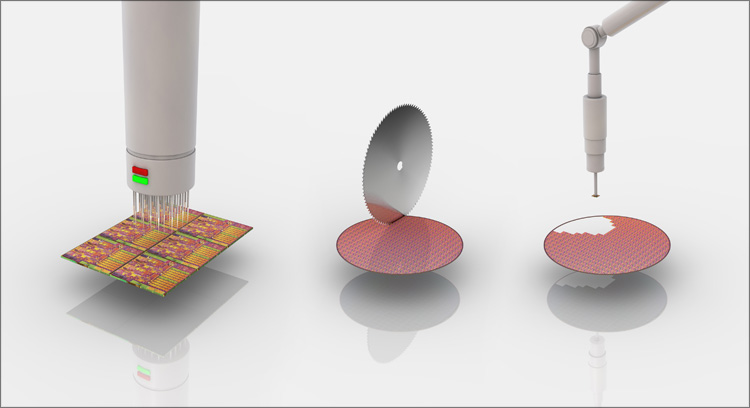
In short, the processor manufacturing process looks like this: a cylindrical single crystal is grown from molten silicon on special equipment. The resulting ingot is cooled and cut into “pancakes”, the surface of which is carefully leveled and polished to a mirror finish. Then, in the "clean rooms" of semiconductor plants on silicon wafers using photolithography and etching techniques, integrated circuits are created. After re-cleaning the plates, laboratory specialists perform a selective testing of processors under a microscope - if everything is OK, then the finished plates are cut into separate processors, which are then enclosed in cases.
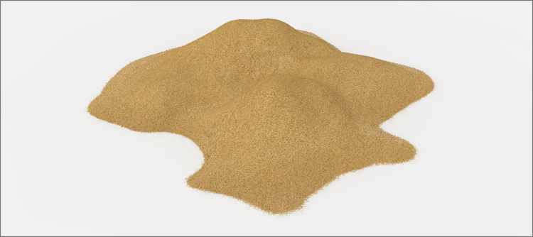
Let's look at the whole process in more detail. The silicon content in the earth's crust is about 25-30% by weight, so that by the prevalence of this element ranks second after oxygen. Sand, especially quartz, has a high percentage of silicon in the form of silicon dioxide (SiO 2 ) and at the beginning of the production process is the basic component for the creation of semiconductors.

Initially, SiO 2 is taken in the form of sand, which in arc furnaces (at a temperature of about 1800 ° C) is reduced by coke:
The ingot is shammed with a “scratch” :) and cut with a diamond saw. At the exit - plates (codename “wafer”) about 1 mm thick and 300 mm in diameter (~ 12 inches; these are exactly what is used for the 32nm process technology with HKMG, High-K / Metal Gate technology). Once upon a time, Intel used disks with a diameter of 50mm (2 "), and in the near future it is already planned to switch to plates with a diameter of 450mm - this is justified at least from the point of view of reducing the cost of chip production. Speaking of saving, all these crystals are grown outside of Intel; for processor production, they are purchased elsewhere.
Each plate is polished, made perfectly smooth, bringing its surface to a mirror shine.
The production of chips consists of more than three hundred operations, as a result of which more than 20 layers form a complex three-dimensional structure - the volume of the article available in Habré does not allow us to briefly mention even half of this list :) Therefore, very briefly and only about the most important stages.
So. It is necessary to transfer the structure of the future processor to the polished silicon wafers, that is, to introduce impurities into certain areas of the silicon wafer, which ultimately form transistors. How to do it? Generally, the application of different layers on the processor base is a whole science, because even in theory such a process is not easy (not to mention practice, given the scale) ... but it’s so nice to understand the complex;) Well, or at least try to figure it out.
The problem is solved with the help of photolithography technology - the process of selective etching of the surface layer using protective photomask. The technology is built on the principle of "light-pattern-photoresist" and is as follows:

Sometimes it is simply impossible to besiege certain materials in the right places on the plate, so it is much easier to put the material on the entire surface at once, removing the excess from those places where it is not needed - the photoresist is shown in the image above in blue.
A plate is irradiated with a stream of ions (positively or negatively charged atoms), which in given places penetrate under the surface of the plate and change the conductive properties of silicon (the green areas are implanted alien atoms).
How to isolate areas that do not require further processing? Before lithography, a dielectric protective film is applied to the surface of a silicon wafer (at high temperature in a special chamber) - as I have already said, Intel began to use a High-K dielectric instead of traditional silicon dioxide. It is thicker than silicon dioxide, but at the same time it has the same capacitive properties. Moreover, due to the increase in thickness, the leakage current through the dielectric is reduced, and as a result, it has become possible to produce more energy-efficient processors. In general, it is much more difficult to ensure the uniformity of this film over the entire surface of the plate - in this regard, high-precision temperature control is used in production.
So here. In those places that will be treated with impurities, a protective film is not needed - it is carefully removed by etching (removing the layer areas to form a multilayer structure with certain properties). And how to remove it not everywhere, but only in the right areas? To do this, it is necessary to apply another layer of photoresist over the film - due to the centrifugal force of the rotating plate, it is applied with a very thin layer.
In the photo, the light passed through the negative film, fell onto the surface of the photo paper and changed its chemical properties. In photolithography, the principle is similar: the light is passed through a photomask to a photoresist, and in those places where it has passed through the mask, certain areas of the photoresist change properties. Light emission is transmitted through the masks, which is focused on the substrate. For precise focusing, a special system of lenses or mirrors is needed that can not only reduce the image cut out on the mask to the size of a chip, but also project it precisely on the workpiece. Printed plates are usually four times smaller than the masks themselves.

The entire spent photoresist (which has changed its solubility under the action of irradiation) is removed with a special chemical solution — part of the substrate dissolves along with the exposed photoresist. The part of the substrate that was masked from light will not dissolve. It forms a conductor or future active element - the result of this approach is a different picture of the closures on each layer of the microprocessor.
As a matter of fact, all the previous steps were necessary in order to create semiconductor structures in necessary places by introducing donor (n-type) or acceptor (p-type) impurities. Suppose we need to make in the silicon a region of p-type carrier concentration, that is, a hole conduction zone. To do this, the plate is processed using a device called an implanter - boron ions with huge energy are fired from a high-voltage accelerator and are evenly distributed in unprotected zones formed by photolithography.
Where the dielectric has been removed, the ions penetrate into the layer of unprotected silicon - otherwise they “get stuck” in the dielectric. After the next etching process, the remains of the dielectric are removed, and on the plate there are zones in which there is boron locally. It is clear that modern processors may have several such layers - in this case, the resulting figure re-grows the dielectric layer and then everything goes along the trodden path - another photoresist layer, the photolithography process (already on the new mask), etching, implantation ... well got it.
The characteristic size of the transistor now is 32 nm, and the wavelength with which silicon is processed is not even ordinary light, but the special ultraviolet excimer laser is 193 nm. However, the laws of optics do not allow the resolution of two objects that are at a distance less than half the wavelength. This happens because of the diffraction of light. How to be? To apply various tricks - for example, in addition to the mentioned excimer lasers, which shine far in the ultraviolet spectrum, modern photolithography uses multi-layer reflective optics using special masks and a special immersion photolithography process.
The logical elements that were formed in the process of photolithography should be connected to each other. To do this, the plates are placed in a copper sulphate solution in which metal atoms "settle" in the remaining "passages" under the action of an electric current - as a result of this galvanic process, conductive regions are formed, creating connections between the individual parts of the processor "logic". Excess conductive coatings are cleaned by polishing.

Hurray - the hardest thing behind. It remains a clever way to connect the "remnants" of transistors - the principle and sequence of all these connections (buses) is called the processor architecture. For each processor, these connections are different - although the schemes appear to be completely flat, in some cases up to 30 levels of such “wires” can be used. Remotely (at a very high magnification) it all looks like a futuristic road junction - and yet someone designs these balls!

When the processing of the plates is completed, the plates are transferred from the production to the assembly and testing workshop. There, the crystals pass the first tests, and those that pass the test (and this is the vast majority) are cut out of the substrate with a special device.
At the next stage, the processor is packaged in a substrate (in the figure, an Intel Core i5 processor consisting of a CPU and an HD graphics chip).

The substrate, the crystal and the heat-spreading lid are connected together - this is the product we will mean by saying the word "processor". The green substrate creates an electrical and mechanical interface (gold is used to electrically connect the silicon chip to the case), thanks to which it will be possible to install the processor into the motherboard socket - in fact, this is just a platform where the contacts from the small chip are separated. The heat distribution cover is a thermal interface that cools the processor during operation - it is this cover that will be adjacent to the cooling system, whether it is a cooler radiator or a healthy water block.
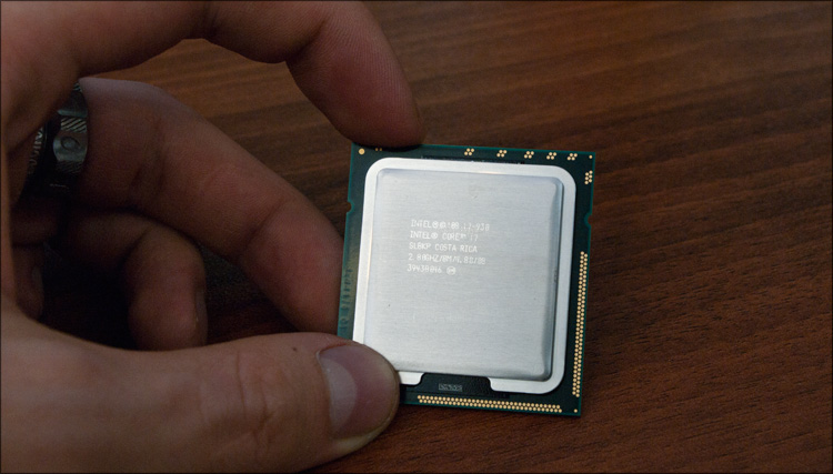

Socket (CPU socket) - socket or slot connector, designed to install the CPU. Using the connector instead of directly decoupling the processor on the motherboard makes it easy to replace the processor for upgrading or repairing the computer. The connector can be designed to install the actual processor or CPU card (for example, in Pegasos). Each slot allows installation of only a certain type of processor or CPU card.

At the final stage of production, ready-made processors pass the final tests for compliance with the basic characteristics - if everything is in order, the processors are sorted in the right order into special trays - in this form, the processors will go to manufacturers or go to an OEM-sale. Another party will go on sale in the form of BOX-versions - in a beautiful box with a stock cooling system.

Now imagine that the company announces, for example, 20 new processors. All of them are different among themselves - the number of cores, cache volumes, supported technologies ... Each processor model uses a certain number of transistors (estimated in millions and even billions), its own principle of connecting elements ... And all this needs to be designed and created / automated - templates, lenses, lithographs, hundreds of parameters for each process, testing ... And all this should work around the clock, in several factories at once ... As a result, devices should appear that do not have the right to make mistakes in working those ... And the cost of these technological masterpieces should be within the bounds of decency ... I am almost sure that you, like me, cannot imagine the whole volume of the work being done, which I tried to tell about today.
Well, something more amazing. Imagine that you are a great scientist without five minutes - you carefully removed the heat-spreading lid of the processor and could see the structure of the processor in a huge microscope - all these connections, transistors ... even sketched something on a piece of paper so as not to forget. Do you think it is easy to learn the principles of the processor, having only this data and data on which tasks can be solved with the help of this processor? It seems to me that about this picture is now visible to scientists who are trying at a similar level to study the work of the human brain. Only according to Stanford microbiologists, are there more “transistors” in one human brain than in the entire global IT infrastructure. Interesting, right?
Enough to read this paragraph? ) Congratulations - it's nice that I tried not in vain. Then I propose to sit back and see everything described above, but in the form of a more visual video - without it, the article would not be complete.
I wrote this article myself, trying to understand the details of the process of processor-building. I mean, there may be some inaccuracies or errors in the article - if you find something, let me know. In general, in order to finally consolidate all the read material and clearly understand what was misunderstood in my article, follow this link . Now for sure.
")
Successes!
As promised - a detailed account of how processors are made ... starting with the sand. Everything you wanted to know, but were afraid to ask)
')
I have already talked about " Where do the processors produce " and about what " Production Difficulties " stand in this way. Today we will speak directly about the production itself - “from and to”.
Processor Manufacture
When a factory for manufacturing processors using a new technology is built, it has 4 years to recoup the investment (over $ 5 billion) and make a profit. From simple secret calculations it turns out that the factory must produce at least 100 working plates per hour.
In short, the processor manufacturing process looks like this: a cylindrical single crystal is grown from molten silicon on special equipment. The resulting ingot is cooled and cut into “pancakes”, the surface of which is carefully leveled and polished to a mirror finish. Then, in the "clean rooms" of semiconductor plants on silicon wafers using photolithography and etching techniques, integrated circuits are created. After re-cleaning the plates, laboratory specialists perform a selective testing of processors under a microscope - if everything is OK, then the finished plates are cut into separate processors, which are then enclosed in cases.
Chemistry lessons
Let's look at the whole process in more detail. The silicon content in the earth's crust is about 25-30% by weight, so that by the prevalence of this element ranks second after oxygen. Sand, especially quartz, has a high percentage of silicon in the form of silicon dioxide (SiO 2 ) and at the beginning of the production process is the basic component for the creation of semiconductors.
Initially, SiO 2 is taken in the form of sand, which in arc furnaces (at a temperature of about 1800 ° C) is reduced by coke:
SiO 2 + 2C = Si + 2COThis silicon is called " technical " and has a purity of 98-99.9%. For the production of processors requires a much cleaner raw materials, called " electronic silicon " - in this should be no more than one foreign atom per billion silicon atoms. To clean up to this level, silicon is literally “reborn”. By chlorination of technical silicon, silicon tetrachloride (SiCl 4 ) is obtained, which is further converted to trichlorosilane (SiHCl 3 ):
3SiCl 4 + 2H 2 + Si 4SiHCl 3These reactions using recycled formed silicon-containing substances reduce the cost and eliminate environmental problems:
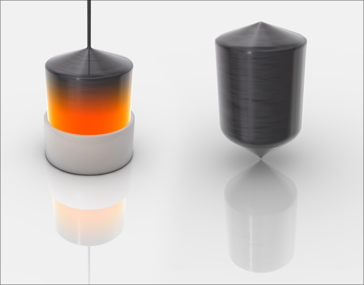
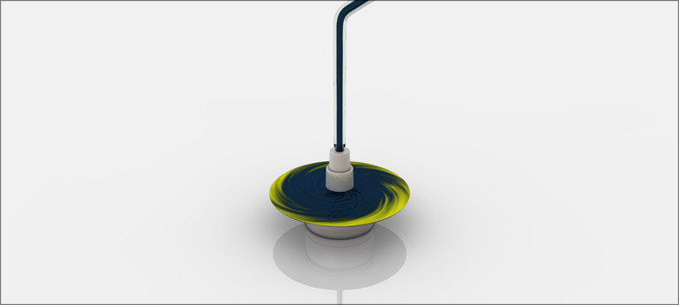
2SiHCl 3 SiH 2 Cl 2 + SiCl 4The resulting hydrogen can be used in many places, but the most important thing is that “electron” silicon was obtained, pure-pure (99.9999999%). A little later, a seed (“growth point”) is lowered into the melt of such silicon, which is gradually drawn out of the crucible. As a result, the so-called “bull” is formed - a single crystal as tall as an adult. The corresponding weight - in the production of such a dule weighs about 100 kg.
2SiH 2 Cl 2 SiH 3 Cl + SiHCl 3
2SiH 3 Cl SiH 4 + SiH 2 Cl 2
SiH 4 Si + 2H 2
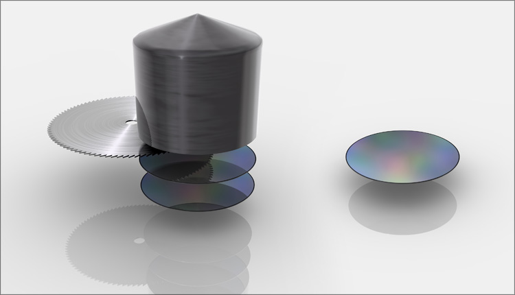
The ingot is shammed with a “scratch” :) and cut with a diamond saw. At the exit - plates (codename “wafer”) about 1 mm thick and 300 mm in diameter (~ 12 inches; these are exactly what is used for the 32nm process technology with HKMG, High-K / Metal Gate technology). Once upon a time, Intel used disks with a diameter of 50mm (2 "), and in the near future it is already planned to switch to plates with a diameter of 450mm - this is justified at least from the point of view of reducing the cost of chip production. Speaking of saving, all these crystals are grown outside of Intel; for processor production, they are purchased elsewhere.
Each plate is polished, made perfectly smooth, bringing its surface to a mirror shine.
The production of chips consists of more than three hundred operations, as a result of which more than 20 layers form a complex three-dimensional structure - the volume of the article available in Habré does not allow us to briefly mention even half of this list :) Therefore, very briefly and only about the most important stages.
So. It is necessary to transfer the structure of the future processor to the polished silicon wafers, that is, to introduce impurities into certain areas of the silicon wafer, which ultimately form transistors. How to do it? Generally, the application of different layers on the processor base is a whole science, because even in theory such a process is not easy (not to mention practice, given the scale) ... but it’s so nice to understand the complex;) Well, or at least try to figure it out.
Photolithography
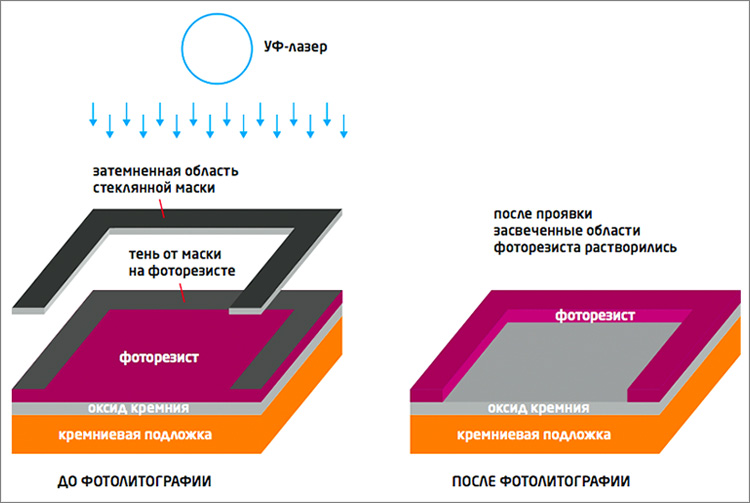
The problem is solved with the help of photolithography technology - the process of selective etching of the surface layer using protective photomask. The technology is built on the principle of "light-pattern-photoresist" and is as follows:
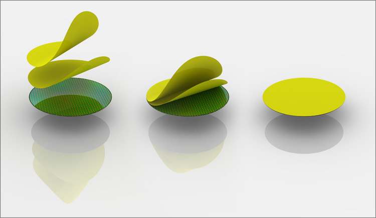
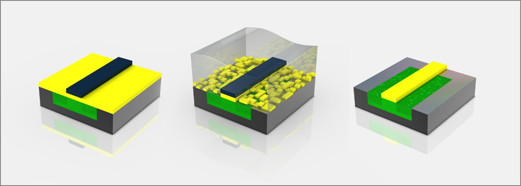
- On a silicon substrate put a layer of material from which you want to form a picture. A photoresist is applied onto it - a layer of polymer-sensitive material that changes its physicochemical properties when irradiated with light.The desired structure is drawn on a photo mask - as a rule, it is a plate made of optical glass, on which opaque areas are photographically applied. Each such template contains one of the layers of the future processor, so it must be very accurate and practical.
- Exposure is performed (illumination of the photo layer for a precisely defined period of time) through the photomask
- Removal of spent photoresist.
Sometimes it is simply impossible to besiege certain materials in the right places on the plate, so it is much easier to put the material on the entire surface at once, removing the excess from those places where it is not needed - the photoresist is shown in the image above in blue.
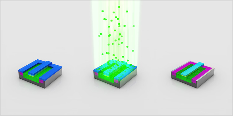
A plate is irradiated with a stream of ions (positively or negatively charged atoms), which in given places penetrate under the surface of the plate and change the conductive properties of silicon (the green areas are implanted alien atoms).
How to isolate areas that do not require further processing? Before lithography, a dielectric protective film is applied to the surface of a silicon wafer (at high temperature in a special chamber) - as I have already said, Intel began to use a High-K dielectric instead of traditional silicon dioxide. It is thicker than silicon dioxide, but at the same time it has the same capacitive properties. Moreover, due to the increase in thickness, the leakage current through the dielectric is reduced, and as a result, it has become possible to produce more energy-efficient processors. In general, it is much more difficult to ensure the uniformity of this film over the entire surface of the plate - in this regard, high-precision temperature control is used in production.
So here. In those places that will be treated with impurities, a protective film is not needed - it is carefully removed by etching (removing the layer areas to form a multilayer structure with certain properties). And how to remove it not everywhere, but only in the right areas? To do this, it is necessary to apply another layer of photoresist over the film - due to the centrifugal force of the rotating plate, it is applied with a very thin layer.
In the photo, the light passed through the negative film, fell onto the surface of the photo paper and changed its chemical properties. In photolithography, the principle is similar: the light is passed through a photomask to a photoresist, and in those places where it has passed through the mask, certain areas of the photoresist change properties. Light emission is transmitted through the masks, which is focused on the substrate. For precise focusing, a special system of lenses or mirrors is needed that can not only reduce the image cut out on the mask to the size of a chip, but also project it precisely on the workpiece. Printed plates are usually four times smaller than the masks themselves.
The entire spent photoresist (which has changed its solubility under the action of irradiation) is removed with a special chemical solution — part of the substrate dissolves along with the exposed photoresist. The part of the substrate that was masked from light will not dissolve. It forms a conductor or future active element - the result of this approach is a different picture of the closures on each layer of the microprocessor.
As a matter of fact, all the previous steps were necessary in order to create semiconductor structures in necessary places by introducing donor (n-type) or acceptor (p-type) impurities. Suppose we need to make in the silicon a region of p-type carrier concentration, that is, a hole conduction zone. To do this, the plate is processed using a device called an implanter - boron ions with huge energy are fired from a high-voltage accelerator and are evenly distributed in unprotected zones formed by photolithography.
Where the dielectric has been removed, the ions penetrate into the layer of unprotected silicon - otherwise they “get stuck” in the dielectric. After the next etching process, the remains of the dielectric are removed, and on the plate there are zones in which there is boron locally. It is clear that modern processors may have several such layers - in this case, the resulting figure re-grows the dielectric layer and then everything goes along the trodden path - another photoresist layer, the photolithography process (already on the new mask), etching, implantation ... well got it.
The characteristic size of the transistor now is 32 nm, and the wavelength with which silicon is processed is not even ordinary light, but the special ultraviolet excimer laser is 193 nm. However, the laws of optics do not allow the resolution of two objects that are at a distance less than half the wavelength. This happens because of the diffraction of light. How to be? To apply various tricks - for example, in addition to the mentioned excimer lasers, which shine far in the ultraviolet spectrum, modern photolithography uses multi-layer reflective optics using special masks and a special immersion photolithography process.
The logical elements that were formed in the process of photolithography should be connected to each other. To do this, the plates are placed in a copper sulphate solution in which metal atoms "settle" in the remaining "passages" under the action of an electric current - as a result of this galvanic process, conductive regions are formed, creating connections between the individual parts of the processor "logic". Excess conductive coatings are cleaned by polishing.
 Finish line
Hurray - the hardest thing behind. It remains a clever way to connect the "remnants" of transistors - the principle and sequence of all these connections (buses) is called the processor architecture. For each processor, these connections are different - although the schemes appear to be completely flat, in some cases up to 30 levels of such “wires” can be used. Remotely (at a very high magnification) it all looks like a futuristic road junction - and yet someone designs these balls!
When the processing of the plates is completed, the plates are transferred from the production to the assembly and testing workshop. There, the crystals pass the first tests, and those that pass the test (and this is the vast majority) are cut out of the substrate with a special device.
At the next stage, the processor is packaged in a substrate (in the figure, an Intel Core i5 processor consisting of a CPU and an HD graphics chip).
Hi, socket!
The substrate, the crystal and the heat-spreading lid are connected together - this is the product we will mean by saying the word "processor". The green substrate creates an electrical and mechanical interface (gold is used to electrically connect the silicon chip to the case), thanks to which it will be possible to install the processor into the motherboard socket - in fact, this is just a platform where the contacts from the small chip are separated. The heat distribution cover is a thermal interface that cools the processor during operation - it is this cover that will be adjacent to the cooling system, whether it is a cooler radiator or a healthy water block.
Socket (CPU socket) - socket or slot connector, designed to install the CPU. Using the connector instead of directly decoupling the processor on the motherboard makes it easy to replace the processor for upgrading or repairing the computer. The connector can be designed to install the actual processor or CPU card (for example, in Pegasos). Each slot allows installation of only a certain type of processor or CPU card.
At the final stage of production, ready-made processors pass the final tests for compliance with the basic characteristics - if everything is in order, the processors are sorted in the right order into special trays - in this form, the processors will go to manufacturers or go to an OEM-sale. Another party will go on sale in the form of BOX-versions - in a beautiful box with a stock cooling system.
The end
Now imagine that the company announces, for example, 20 new processors. All of them are different among themselves - the number of cores, cache volumes, supported technologies ... Each processor model uses a certain number of transistors (estimated in millions and even billions), its own principle of connecting elements ... And all this needs to be designed and created / automated - templates, lenses, lithographs, hundreds of parameters for each process, testing ... And all this should work around the clock, in several factories at once ... As a result, devices should appear that do not have the right to make mistakes in working those ... And the cost of these technological masterpieces should be within the bounds of decency ... I am almost sure that you, like me, cannot imagine the whole volume of the work being done, which I tried to tell about today.
Well, something more amazing. Imagine that you are a great scientist without five minutes - you carefully removed the heat-spreading lid of the processor and could see the structure of the processor in a huge microscope - all these connections, transistors ... even sketched something on a piece of paper so as not to forget. Do you think it is easy to learn the principles of the processor, having only this data and data on which tasks can be solved with the help of this processor? It seems to me that about this picture is now visible to scientists who are trying at a similar level to study the work of the human brain. Only according to Stanford microbiologists, are there more “transistors” in one human brain than in the entire global IT infrastructure. Interesting, right?
 BONUS
BONUS
Enough to read this paragraph? ) Congratulations - it's nice that I tried not in vain. Then I propose to sit back and see everything described above, but in the form of a more visual video - without it, the article would not be complete.
I wrote this article myself, trying to understand the details of the process of processor-building. I mean, there may be some inaccuracies or errors in the article - if you find something, let me know. In general, in order to finally consolidate all the read material and clearly understand what was misunderstood in my article, follow this link . Now for sure.
Successes!
Source: https://habr.com/ru/post/110234/
All Articles