Saving and restoring media player firmware from Vogue magazine
Experimenting with a player from Vogue magazine is very good, but the good old admin's habit of making backups of everything and everything bothers me. For it is very easy to spoil a toy when experimenting with other people's firmware, and how to return it to its original state is not clear. It would be a shame to spoil such a freebie.
So after a 3-day brainstorming on this device, I have thoroughly disassembled the process of saving the native firmware and flooding it back. Special thanks to tronix286 for modifying the original usb_boot program, adding the ability to read the firmware to the file, and for throwing a couple of useful datasheets.
Everything you need to reflash and restore the player to its original state is here .
Actually in the archive there is a working and configured usb-boot version for the log + firmware files.
For the most impatient I will immediately describe the recovery process:
- disconnect the battery from the player, or insert a piece of paper under the contact of the opening page;
- press the button on the player and with the button pressed, insert the usb cable and release the button;
-computer defines a new device, install drivers for it from the archive, the device icon remains in the form of a question, but don’t be alarmed;
- run usb_boot.exe;
- enter the “run restore.sh” command there and the recovery process started.
')
If errors are sprinkled in the recovery process, either we use a shorter usb cable or it must be plugged into the connector on the back of the computer. We eliminate the problem with the cable and try everything on a new one.
Actually after that we get the working device again. (Impatient and not curious can finish reading =))
Now I’ll tell you more about the process of saving / restoring the player’s firmware and about its components.
Before we go into all serious things, we must understand what we are dealing with.
Firmware and user content in the player is stored in the NAND-flash chip of the Samsung K9G8G08U0A memory.
NAND-flash memory chips are generally a very peculiar thing and have their own, at first not familiar to ordinary computer scientists, the organization of memory space and the size of sectors / blocks. Let's try to figure it out.
The minimum addressable unit in this type of memory is a page (a kind of sector / block analogue of a hard disk). The page itself has, at first glance, a strange size of 528/1056/2112/4224/8448 ... bytes, depending on the model. But it is made of good intentions. NAND-flash memory has a very limited number of write cycles and over time its individual bits begin to fail. To identify these failures and restore information in the page with bad bits, such an “exotic” size was chosen. The page is essentially divided into two parts. The first part 512/1024/2048/4096/8192 ... bytes is a multiple of 512 bytes and stores user information, and in the remaining part 16/32/64/128 ... 256 bytes the ECC (checksum) of the first part of the page and some other service information. When each page is read, the subsequent calculation of its ECC occurs and the verification with the previously recorded one, in case of non-coincidence the page is recognized as failed and its value is restored by the read ECC.
Next, the pages are combined into blocks. This is done at the hardware level to speed up the process of erasing information in all pages of the block with a single command. Next, the blocks are physically combined into one silicon crystal. Such crystals in one package can be 1, 2 or 4 and they are selected using the CS (chip select) terminals.
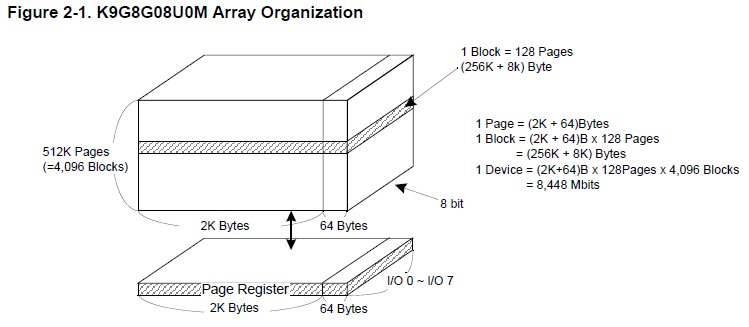
Now back to our experimental K9G8G08U0A. Its memory organization is as follows: 2048 + 64 bytes per page, 128 pages in a block and 4096 blocks in a chip.
To simplify the understanding of the above, here is a picture of the official datasheet on this chip:
Having understood the organization of memory chips, we consider the component parts of the firmware and the process of running the hardware OS
The firmware consists of the following parts (see the * .bin files in the folder with the flasher):
1) spl (secondary program loader) - initial loader, file nand.bin in the archive
2) loader - the main loader itself, which loads the OS kernel into memory and transfers control to it, the loader.bin file
3) loader config - bootloader settings, where the location of the OS kernel and resources in the NAND chip and the addresses in the RAM for which all this is loaded is specified, the def_boot.bin file
4) boot image - the image that is displayed when the OS is loaded (yes, that is the yellow one), img_boot.bin file
5) MINIOS kernel, minios.bin file
6) OS internal file system with various resources, res.bin file.
Actually in the same sequence and the launch of the OS.
First of all, the IPL starts (the boot loader is wired by the manufacturer into the processor itself). It checks the condition of the processor legs, which set the boot sequence and whether the button is pressed. If the button is pressed, then loading via USB is expected, if not, then it is loading from memory. The IPL reads the first 8 kilobytes (0-3 pages) containing the SPL code of the bootloader into the internal SRAM memory from the NAND-flash memory microchip. It checks their correctness by ECC and some other signs, and if everything is fine, it transfers control to it. If something went wrong, then a similar action is performed with the next 8 kilobytes of NAND-flash memory (4-7 pages).
After the start, SPL initializes the registers and peripherals of the processor, configures the SDRAM controller and loads into the RAM the code of the OS direct loader (loader.bin) at the address specified at the beginning of 61 and 62 pages.
Then the main loader loads the core of the operating system into RAM and transfers control to it.
The question arises, why should there be so many loaders? There's nothing you can do about it, iron constraint. IPL can not load more than 8 kilobytes of code, so you have to make a 2-storey bootloader.
From the theoretical foundations proceed to practice
Let's look athow it works, this damned moonshine! ... eeee, in the sense of how the utility is designed to download the player via USB and its firmware.
-fw.bin and usb_boot.bin files are, nothing else, written in a special way by SPL and Loader;
programs USB_Boot.exe - the original management utility spec. loader usb_boot.bin, Test_jz4740_usb.exe - corrected tronix286th version with the ability to read the contents of NAND-flash memory to a file;
- all other files * .bin - player firmware components;
files Usb_Boot_Driver.inf and Usb_Boot_Driver.sys - drivers for the player in usb-boot mode;
-files * .cfg - bootloader configuration files for different memory chips (both NAND and SDRAM) and their modes of operation.
-file restore.sh - script for uploading firmware to the player.
The Test_jz4740_usb.exe utility differs from USB_Boot.exe in the presence of two commands (ndump and nreadtofile) for reading firmware from the player’s memory.
The commands that we need:
-boot - download the usb-loader to the player using the default configuration from the USBBoot.cfg file
-nerase - ON BLOCK erasing information from a NAND-flash memory chip;
-nprog - write information from a file to the pages of a NAND-flash memory chip;
-ndump - read the contents of memory from NAND-flash to a file;
-fconfig - switch configurations.
The parameters of each command can be found by running it without parameters.
Let's figure out how to keep the original firmware
Immediately I will tell about one huge nuance, about which a heap of copies was broken and a dozen swords were blunted in the process of brainstorming. SPL is loaded and readable with the USBBoot_nand.cfg configuration, and everything else with the USBBoot_norm.cfg configuration. The use of 2 configs is due to the fact that the spl-loader and the rest are recorded with different formats of the service area (in terms of usb-boot it is called OOB) and the page checksum. For the SPL loader, the format used is iron wired inside the processor, and for everything else, the one chosen by the programmers during the build and compilation of the loader and the OS.
Before you start saving native firmware, do not forget to delete files with my firmware from the folder. To merge the firmware do the following:
- disconnect the battery from the player, or insert a piece of paper under the contact of the opening page;
- press the button on the player and with the button pressed, insert the usb cable and release the button;
-computer determines the new device, install drivers for it from the archive;
-start Test_jz4740_usb.exe;
- enter the " boot 0 " command, and look at the result of its execution. Something like this should appear:
- switch to the “correct” configuration for reading SPL with the command " fconfig USBBoot_nand.cfg 0 ", again if everything is in order there should be an inscription "
- we read SPL and its configuration pages in the nand.bin file with the command " ndump 0 64 0 0 nand.bin ";
- switch to the “correct” configuration for reading the rest of the firmware with the command " fconfig USBBoot_norm.cfg 0 ", if everything is in order, the message "
- read the loader in the file loader.bin with the command " ndump 128 66 0 0 loader.bin "
-we read its settings in the file def_boot.bin with the command " ndump 256 1 0 0 def_boot.bin "
- read the boot image to the file img_boot.bin with the command " ndump 512 3061 0 0 img_boot.bin "
- read the OS kernel into the minios.bin file with the command " ndump 8192 8192 0 0 minios.bin "
- read the internal file system with the kernel resources in the res.bin file with the command " ndump 32768 32768 0 0 res.bin ".
If desired, all these commands in turn can be written to a file and started with the run command as well as the fill process. UPD. Which I did and saved to the save.sh file.
The resulting files are the backup of the native firmware. Now with the firmware of the player you can do anything and are not afraid to get a worthless piece of hardware.
All the addresses for recording were obtained from the information that displays on the player's internal uart-ovu console when loading and experimentally.
As a result, we obtain:
1) SPL is in 0-3 pages;
2) 61, 62, 63 pages need SPL for later download;
3) the main loader starts with 128 pages;
4) its configuration is 256 pages;
5) the boot image starts from 512 pages;
6) MINIOS core starts from 8192 pages;
7) internal FS starts 32768 pages;
8) further follows the user file system with content.
The process of uploading the firmware back to the player I think it is unnecessary to comment, it is similar to saving. If you open the restore.sh file with a notepad (or any other text editor), you can see all the commands of the process with your own eyes. If you wish, you can not completely flash the player, and only change its individual parts.
Now, having a backup firmware and knowing how to fill it, you can try to pour into the player any other firmware. At the moment I am trying to compile and write the u-boot bootloader into it to run Linux.
UPD !!! In the utility Test_jz4740_usb.exe, an annoying error was found! Be sure to download the archive again with the latest version of the utility at the link at the beginning of the post or separately the utility itself is here !
All old archives have been deleted, in order to avoid the spread of glitches.
So after a 3-day brainstorming on this device, I have thoroughly disassembled the process of saving the native firmware and flooding it back. Special thanks to tronix286 for modifying the original usb_boot program, adding the ability to read the firmware to the file, and for throwing a couple of useful datasheets.
Everything you need to reflash and restore the player to its original state is here .
Actually in the archive there is a working and configured usb-boot version for the log + firmware files.
For the most impatient I will immediately describe the recovery process:
- disconnect the battery from the player, or insert a piece of paper under the contact of the opening page;
- press the button on the player and with the button pressed, insert the usb cable and release the button;
-computer defines a new device, install drivers for it from the archive, the device icon remains in the form of a question, but don’t be alarmed;
- run usb_boot.exe;
- enter the “run restore.sh” command there and the recovery process started.
')
If errors are sprinkled in the recovery process, either we use a shorter usb cable or it must be plugged into the connector on the back of the computer. We eliminate the problem with the cable and try everything on a new one.
Actually after that we get the working device again. (Impatient and not curious can finish reading =))
Now I’ll tell you more about the process of saving / restoring the player’s firmware and about its components.
Before we go into all serious things, we must understand what we are dealing with.
Firmware and user content in the player is stored in the NAND-flash chip of the Samsung K9G8G08U0A memory.
NAND-flash memory chips are generally a very peculiar thing and have their own, at first not familiar to ordinary computer scientists, the organization of memory space and the size of sectors / blocks. Let's try to figure it out.
The minimum addressable unit in this type of memory is a page (a kind of sector / block analogue of a hard disk). The page itself has, at first glance, a strange size of 528/1056/2112/4224/8448 ... bytes, depending on the model. But it is made of good intentions. NAND-flash memory has a very limited number of write cycles and over time its individual bits begin to fail. To identify these failures and restore information in the page with bad bits, such an “exotic” size was chosen. The page is essentially divided into two parts. The first part 512/1024/2048/4096/8192 ... bytes is a multiple of 512 bytes and stores user information, and in the remaining part 16/32/64/128 ... 256 bytes the ECC (checksum) of the first part of the page and some other service information. When each page is read, the subsequent calculation of its ECC occurs and the verification with the previously recorded one, in case of non-coincidence the page is recognized as failed and its value is restored by the read ECC.
Next, the pages are combined into blocks. This is done at the hardware level to speed up the process of erasing information in all pages of the block with a single command. Next, the blocks are physically combined into one silicon crystal. Such crystals in one package can be 1, 2 or 4 and they are selected using the CS (chip select) terminals.
Now back to our experimental K9G8G08U0A. Its memory organization is as follows: 2048 + 64 bytes per page, 128 pages in a block and 4096 blocks in a chip.
To simplify the understanding of the above, here is a picture of the official datasheet on this chip:
Having understood the organization of memory chips, we consider the component parts of the firmware and the process of running the hardware OS
The firmware consists of the following parts (see the * .bin files in the folder with the flasher):
1) spl (secondary program loader) - initial loader, file nand.bin in the archive
2) loader - the main loader itself, which loads the OS kernel into memory and transfers control to it, the loader.bin file
3) loader config - bootloader settings, where the location of the OS kernel and resources in the NAND chip and the addresses in the RAM for which all this is loaded is specified, the def_boot.bin file
4) boot image - the image that is displayed when the OS is loaded (yes, that is the yellow one), img_boot.bin file
5) MINIOS kernel, minios.bin file
6) OS internal file system with various resources, res.bin file.
Actually in the same sequence and the launch of the OS.
First of all, the IPL starts (the boot loader is wired by the manufacturer into the processor itself). It checks the condition of the processor legs, which set the boot sequence and whether the button is pressed. If the button is pressed, then loading via USB is expected, if not, then it is loading from memory. The IPL reads the first 8 kilobytes (0-3 pages) containing the SPL code of the bootloader into the internal SRAM memory from the NAND-flash memory microchip. It checks their correctness by ECC and some other signs, and if everything is fine, it transfers control to it. If something went wrong, then a similar action is performed with the next 8 kilobytes of NAND-flash memory (4-7 pages).
After the start, SPL initializes the registers and peripherals of the processor, configures the SDRAM controller and loads into the RAM the code of the OS direct loader (loader.bin) at the address specified at the beginning of 61 and 62 pages.
Then the main loader loads the core of the operating system into RAM and transfers control to it.
The question arises, why should there be so many loaders? There's nothing you can do about it, iron constraint. IPL can not load more than 8 kilobytes of code, so you have to make a 2-storey bootloader.
From the theoretical foundations proceed to practice
Let's look at
-fw.bin and usb_boot.bin files are, nothing else, written in a special way by SPL and Loader;
programs USB_Boot.exe - the original management utility spec. loader usb_boot.bin, Test_jz4740_usb.exe - corrected tronix286th version with the ability to read the contents of NAND-flash memory to a file;
- all other files * .bin - player firmware components;
files Usb_Boot_Driver.inf and Usb_Boot_Driver.sys - drivers for the player in usb-boot mode;
-files * .cfg - bootloader configuration files for different memory chips (both NAND and SDRAM) and their modes of operation.
-file restore.sh - script for uploading firmware to the player.
The Test_jz4740_usb.exe utility differs from USB_Boot.exe in the presence of two commands (ndump and nreadtofile) for reading firmware from the player’s memory.
The commands that we need:
-boot - download the usb-loader to the player using the default configuration from the USBBoot.cfg file
-nerase - ON BLOCK erasing information from a NAND-flash memory chip;
-nprog - write information from a file to the pages of a NAND-flash memory chip;
-ndump - read the contents of memory from NAND-flash to a file;
-fconfig - switch configurations.
The parameters of each command can be found by running it without parameters.
Let's figure out how to keep the original firmware
Immediately I will tell about one huge nuance, about which a heap of copies was broken and a dozen swords were blunted in the process of brainstorming. SPL is loaded and readable with the USBBoot_nand.cfg configuration, and everything else with the USBBoot_norm.cfg configuration. The use of 2 configs is due to the fact that the spl-loader and the rest are recorded with different formats of the service area (in terms of usb-boot it is called OOB) and the page checksum. For the SPL loader, the format used is iron wired inside the processor, and for everything else, the one chosen by the programmers during the build and compilation of the loader and the OS.
Before you start saving native firmware, do not forget to delete files with my firmware from the folder. To merge the firmware do the following:
- disconnect the battery from the player, or insert a piece of paper under the contact of the opening page;
- press the button on the player and with the button pressed, insert the usb cable and release the button;
-computer determines the new device, install drivers for it from the archive;
-start Test_jz4740_usb.exe;
- enter the " boot 0 " command, and look at the result of its execution. Something like this should appear:
Checking state of No.0 device: Unboot
Now booting No.0 device: START_ADDR 2000000 81c00000

Download stage one program and execute at 0x80002000: Pass
Download stage two program and execute at 0x81c00000: Pass
Boot success!
Now configure No.0 device:
Now checking whether all configure args valid:
Current device information: CPU is Jz4750
Crystal work at 12MHz, the CCLK up to 336MHz and PMH_CLK up to 112MHz
Total SDRAM size is 32 MB, work in 4 bank and 16 bit mode
Nand page size 2048, ECC offset 3, bad block ID 0, use 1 plane mode
Configure success!
- switch to the “correct” configuration for reading SPL with the command " fconfig USBBoot_nand.cfg 0 ", again if everything is in order there should be an inscription "
Configure success! ";- we read SPL and its configuration pages in the nand.bin file with the command " ndump 0 64 0 0 nand.bin ";
- switch to the “correct” configuration for reading the rest of the firmware with the command " fconfig USBBoot_norm.cfg 0 ", if everything is in order, the message "
Configure success! " should be;- read the loader in the file loader.bin with the command " ndump 128 66 0 0 loader.bin "
-we read its settings in the file def_boot.bin with the command " ndump 256 1 0 0 def_boot.bin "
- read the boot image to the file img_boot.bin with the command " ndump 512 3061 0 0 img_boot.bin "
- read the OS kernel into the minios.bin file with the command " ndump 8192 8192 0 0 minios.bin "
- read the internal file system with the kernel resources in the res.bin file with the command " ndump 32768 32768 0 0 res.bin ".
If desired, all these commands in turn can be written to a file and started with the run command as well as the fill process. UPD. Which I did and saved to the save.sh file.
The resulting files are the backup of the native firmware. Now with the firmware of the player you can do anything and are not afraid to get a worthless piece of hardware.
All the addresses for recording were obtained from the information that displays on the player's internal uart-ovu console when loading and experimentally.
As a result, we obtain:
1) SPL is in 0-3 pages;
2) 61, 62, 63 pages need SPL for later download;
3) the main loader starts with 128 pages;
4) its configuration is 256 pages;
5) the boot image starts from 512 pages;
6) MINIOS core starts from 8192 pages;
7) internal FS starts 32768 pages;
8) further follows the user file system with content.
The process of uploading the firmware back to the player I think it is unnecessary to comment, it is similar to saving. If you open the restore.sh file with a notepad (or any other text editor), you can see all the commands of the process with your own eyes. If you wish, you can not completely flash the player, and only change its individual parts.
Now, having a backup firmware and knowing how to fill it, you can try to pour into the player any other firmware. At the moment I am trying to compile and write the u-boot bootloader into it to run Linux.
UPD !!! In the utility Test_jz4740_usb.exe, an annoying error was found! Be sure to download the archive again with the latest version of the utility at the link at the beginning of the post or separately the utility itself is here !
All old archives have been deleted, in order to avoid the spread of glitches.
Source: https://habr.com/ru/post/109265/
All Articles