The difficulties of manufacturing processors
Recently in Moscow Polytechnic Museum the computer equipment stand has been seriously updated - Intel has placed its stand there, which was called " From sand to processor ". From now on, this stand will become an integral part of school trips, but even I advise adults not to postpone visiting the institution for more than five years - by 2016, Intel plans to seriously upgrade the museum so that it can enter the top ten science museums in the world!
A cycle of lectures of the same name in three parts was timed to this event. Two lectures have already passed - you can find their content under the cut. Well, if you are interested in all this, you will still have time to attend the third lecture, information about which is at the end of the post.
I am not ashamed to admit that most of this text is indeed a summary of the first lecture given by Nikolay Suetin , director of external projects in the field of research and development of Intel in Russia. For the most part, it was about modern semiconductor technology and the problems that they face.
')
I propose to start reading interesting, and we start with the basics.
 Technically, a modern microprocessor is designed as a single ultra-large integrated circuit consisting of several billion elements - this is one of the most complex structures created by man. The key elements of any microprocessor are discrete switches - transistors. By blocking and passing electric current (on-off), they enable computer logic circuits to operate in two states, that is, in a binary system. The sizes of transistors are measured in nanometers. One nanometer (nm) is one billionth (10−9) of a meter.
The main part of the work when creating processors is done not by people at all, but by robotic mechanisms - it is they who carry silicon plates to and fro. The production cycle of each plate can be up to 2-3 months.
In more detail (and clearly) about the technology of production of processors, I will tell, but for now, quite briefly.
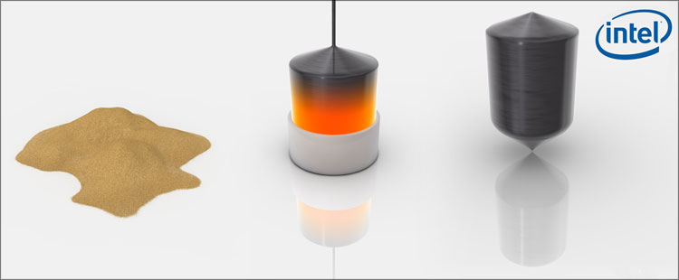
The plates are really made of sand - silicon is the second most common oxygen after the prevalence in the earth's crust. By chemical reactions, silicon oxide (SiO 2 ) is thoroughly cleaned, making “dirty” clean. For microelectronics need monocrystalline silicon - it is obtained from the melt. It all starts with a small crystal (which is lowered into the melt) - later it turns into a special single-crystal “boule” of human growth. Then the main defects are removed and special boules (with diamond powder) boules are cut into discs - each disc is carefully processed to an absolutely flat and smooth (at the atomic level) surface. The thickness of each plate is about 1 mm - solely so that it does not break or bend, that is, so that you can work comfortably with it.
The diameter of each plate is exactly 300mm - a bit later hundreds or even thousands of processors will “grow” on this area. By the way, Intel, Samsung, Toshiba and TSMC have already announced that they are developing equipment capable of working with 450mm plates (more processors will fit on a larger area, and therefore the price of each will be lower) - they will be switched to 2012
Here is a cross-sectional image of the processor:
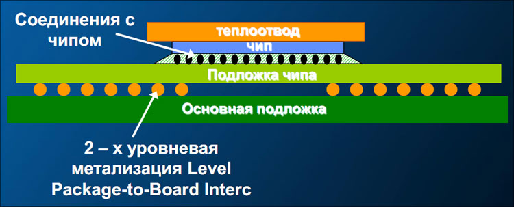
There is a protective metal lid on top, which besides the protective function, also acts as a heat spreader - it is this we abundantly smear with thermal paste when we install the cooler. Under the heat spreader is the same piece of silicon that performs all user tasks. Even lower is a special substrate that is needed for the wiring of contacts (and increasing the area of the “legs”) so that the processor can be installed in the socket of the motherboard.
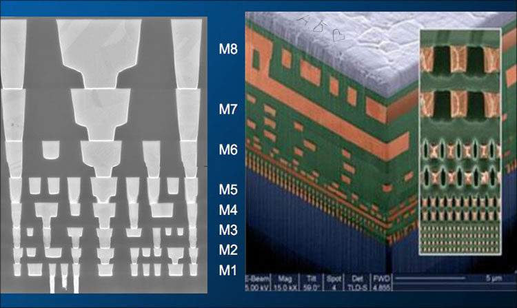
The chip itself consists of silicon, on which there are up to 9 metallization layers (of copper) —that is how many levels are needed so that, according to a certain law, it is possible to connect transistors located on the surface of silicon (since it is simply impossible to do all this at the same level). In fact, these layers act as connecting wires, only on a much smaller scale; so that the “wires” do not short-circuit each other, they are separated by a layer of oxide (with a low dielectric constant).
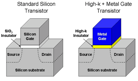
As I wrote above, the unit cell of the processor is a field effect transistor. The first semiconductor products were from Germany and the first transistors were made from it. But as soon as they began to make field-effect transistors (under the gate of which there is a special insulating layer - a thin dielectric film that controls the "on" and "off" of the transistor), germanium immediately became "extinct", giving way to silicon. For the last 40 years, silicon dioxide (SiO 2 ) has been used as the main material for the gate dielectric, which was due to its manufacturability and the possibility of systematically improving the characteristics of transistors as their sizes decrease.
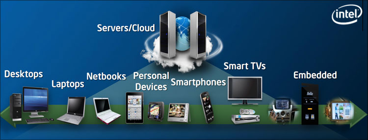
The scaling rule is simple - reducing the size of the transistor, the thickness of the dielectric should decrease proportionally. For example, in chips with a 65nm process technology, the thickness of the dielectric layer of the gate of SiO 2 was about 1.2 nm, which is equivalent to five atomic layers. In fact, this is the physical limit for this material, since as a result of further reduction of the transistor itself (and hence the reduction of the silicon dioxide layer), the leakage current through the gate dielectric increases significantly, which leads to significant current losses and excessive heat generation. In this case, the layer of silicon dioxide ceases to be an obstacle to quantum tunneling of electrons, because of which the possibility of guaranteed control of the state of the transistor is lost. Accordingly, even with the ideal production of all transistors (the number of which in a modern processor reaches several billions), incorrect operation of at least one of them means incorrect operation of all processor logic, which can easily lead to a catastrophe - if we consider that microprocessors control the operation all digital devices (from modern cell phones to car fuel systems).
The process of miniaturization of transistors did not go contrary to the laws of physics, but computer progress, as we see, did not stop. This means that the problem with the dielectric is somehow solved. And they really decided - when switching to 45nm, Intel began to use a new material, the so-called high-k dielectric, which replaced the hopelessly thin layer of silicon dioxide. The layer based on the rare earth metal oxide hafnium with a high (20 vs. 4 in SiO 2 ) dielectric constant k (high-k) became thicker, but this reduced the leakage current by more than ten times, while retaining the ability to correctly and stably manage transistor operation. The new dielectric proved to be poorly compatible with the polysilicon gate, but even this did not become an obstacle - to increase the speed, the gate in the new transistors was made of metal.
Thus, Intel became the first company in the world to switch to the mass production of microprocessors using hafnium. Moreover, the palm is still owned by the corporation - so far no one can reproduce this technology, because the dielectric film is created by atomic sputtering, and the material is applied in successive layers with a thickness of only one atom.
Interestingly, after reading these paragraphs did you have a thought about how billions of transistors design, make and fit on such a small area? And how does it all work in the end and, at the same time, it costs quite reasonable money? I became very thoughtful, although I had previously considered all this obvious and I even had the conscience to think, “ Hey, why is it so expensive? For one processor only! ":)
In 1965, one of the founders of Intel, Gordon Moore, recorded empirical observation, which later became the famous law of his name. Presenting as a graph the performance improvement of memory microcircuits, he found a curious regularity: new microcircuit models were developed after equal periods of time — approximately 18–24 months — after the appearance of their predecessors, and the capacity of the microcircuits doubled each time.

Later, Gordon Moore predicted the pattern, assuming that the number of transistors in microprocessors will double every two years - in fact, constantly creating innovative technologies, Intel has been implementing Moore’s law for more than 40 years.
The number of transistors continues to grow, although the size of the processor "at the output" remains relatively unchanged. Again, there is no secret - it becomes clear if you look at the following dependency.
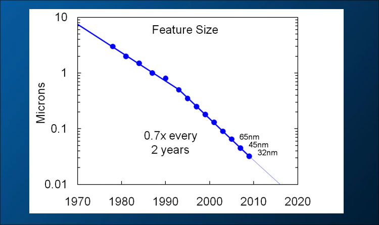
As you can see, every two years the topological dimensions are reduced by a factor of 0.7. As a result of reducing the size of transistors - their switching speed is higher, the price is lower and power consumption is lower.
Currently, Intel is releasing 32nm processors. Key technical differences from 45nm technology:
- 9 levels of plating are used
- a high-k dielectric of the new generation is used (also hafnium oxide, but with special additives - the resulting layer is equivalent to 0.9 nm of silicon oxide)
Creating a new process to create a metal gate led to a 22% increase in the performance of all transistors (compared to 45nm), as well as to the highest density of elements, which required the highest current density.
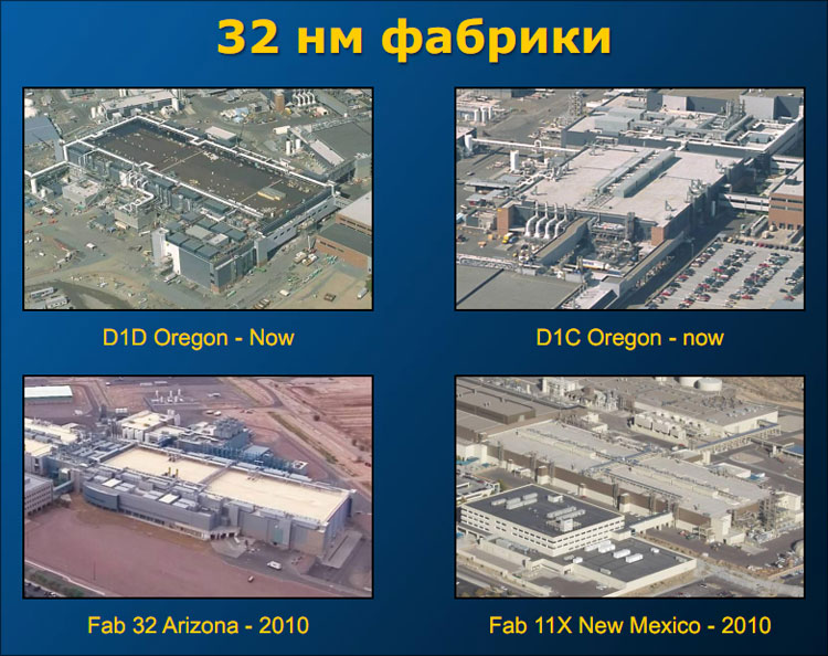
Intel manufactures processors in three countries — the United States, Israel, and Ireland. At the moment, the company has 4 factories for the mass production of processors using 32nm technology. These are: D1D and D1C in Oregon, Fab 32 in Arizona and Fab 11X in New Mexico. There are many interesting things in the structure of these plants and in their work, but I will tell you about it next time.
The cost of such a plant is about $ 5 billion, and if you make several plants at once, then the amount of investment can be easily multiplied. If we consider that the change of technology occurs once every two years, it turns out that the plant has exactly 4 years to “discourage” the $ 5 billion invested in it and make a profit. From which the obvious conclusion suggests itself - the economy very much dictates the development of technical progress ... but, despite all these huge figures, the cost of producing one transistor continues to fall - now it is less than one billion dollars.
No need to think that with the transition of several factories to 32nm, all of a sudden it will be produced by this technical process - the same chipsets and other peripheral circuits simply do not need it - in most cases they use 45nm. The frontier at 22nm is planned to be fully taken next year, and by 2013 it will most likely be 16nm. At least, this year a test plate (at 22nm) was already made, on which the performance of all the elements necessary for the operation of the processor was demonstrated.
* UPD from nE0 * The need to reduce the thickness of the gate dielectric is dictated by the simple formula of a flat capacitor:
 The gate area of the transistor is reduced, and for the transistor to work, the capacitance of the gate dielectric needs to be maintained.
Therefore, it was necessary to reduce its thickness, and when it became impossible to find a material with a higher dielectric constant.
When will the era of silicon end? The exact date is still unknown, but it is definitely not far off. In the 22nm technology, it will still definitely “fight”, most likely it will remain in 16nm ... but then the most interesting things will begin. The periodic table, in principle, is quite large and there is something to choose from) But, most likely, everything will rest not only in chemistry. Increasing the efficiency of the processor can be achieved either by reducing the topological dimensions (they are doing this now), or by using other compounds with higher carrier mobility — perhaps gallium arsenide, possibly “sensational” and promising graphene (by the way, its mobility is hundreds of times higher than that of silicon). But there are problems here. Now technologies are designed for processing plates with a diameter of 300mm - the amount of gallium arsenide needed for such a plate is simply not in nature, and graphene (the Word insistently suggests writing a “decanter”) of this size is still extremely difficult to do - learned to do it, but many defects and problems reproduction, doping, etc.
Most likely, the next step will be the deposition of single-crystal gallium arsenide on silicon, but then already graphene. And, perhaps, the development of microelectronics will go not only along the path of improving technologies, but also along the path of developing fundamentally new logic - this, too, cannot be ruled out. Let's bet, gentlemen? ;)
In general, now there is a struggle for technology and high mobility. But one thing is clear - there is no reason to stop progress.
The process of manufacturing processors consists of two large "parts". For the first, you need to have the manufacturing technology itself, and for the second, you need an understanding of WHAT to manufacture and how - the architecture (how the transistors are connected). If both the new architecture and the new technology are made, then in case of failure it will be difficult to find the "guilty" - some will say that the "architects" are to blame, others - that the technologists. In general, to follow this strategy is very short-sighted.
At Intel, the introduction of a new technology and architecture is separated in time - technology is introduced in one year (and the already developed architecture is produced using a new technology - if something goes wrong, technology will be to blame); and when the new technology will be worked out - the architects will make a new architecture for it, and if something does not work on the developed technology, then the architects will be guilty. This strategy was called "Tick-Tack".
More clearly:
With the current pace of technology development, fantastic investment in research and development is required - Intel annually invests $ 4-5 billion in this business. Part of the work takes place within the company, but a lot is outside it. It’s almost impossible to just keep the whole lab in the company like Bell Labs (the forge of Nobel laureates).
As a rule, the first ideas are laid in universities - in order for universities to know exactly what it makes sense to work (what technologies are in demand and what will be relevant), all the “semiconductor companies” were united into a consortium. After that, they provide a kind of roadmap - it talks about all the problems that will face the semiconductor industry in the next 3-5-7 years. In theory, any company has the right to literally go to the university and “take advantage” of one or another innovation, but the rights to them, as a rule, remain with the university developer — this approach is called “open innovation.” Intel is not an exception and periodically listens to the ideas of students - after protection, selection at the engineering level and testing in real conditions, the idea has every chance to become a new technology.
Here is a list of research centers around the world with which Intel works (except for universities):

Increased productivity leads to higher prices for factories, and this in turn leads to natural selection. For example, to pay for itself in 4 years, each Intel factory must produce at least 100 working wafers per hour. There are thousands of chips on each plate ... and if you make certain calculations, it will become clear - if Intel did not have 80% of the global processor market, the company simply could not recoup the costs. The conclusion is that owning our own "design" and our own production in our time is quite expensive - at least you need to have a huge market. The result of natural selection can be seen below - as you can see, fewer and fewer companies keep pace with technical progress with their “design” and production. Everyone else had to switch to fabless mode - for example, neither Apple, nor NVIDIA, nor even AMD has its own factories and they have to use the services of other companies.
In addition to Intel, only two companies are potentially ready for 22nm technology worldwide - Samsung and TSMC, which invested more than $ 1 billion in their factories last year. Moreover, TSMC does not have its own design division (only foundry) - in fact, it’s just a high-tech forge that takes orders from other companies and often doesn’t even know what it is forging.
As you can see, natural selection was quite fast - in just 3 years. Two conclusions can be drawn from here. The first is that without your factory the industry leader is unlikely to succeed; the second - in fact, you can succeed without your plant. By and large, there is enough of a good computer, brains and the ability to “draw” - the threshold for entering the market has greatly decreased and it is for this reason that a lot of startups have appeared. Someone comes up with a certain scheme for which there is or is artificially created a certain market - novice manufacturers rise ... PROFIT! But here the threshold to the foundry market has risen strongly and will continue to grow ...
What else has changed in recent years? If you recall, then the year until 2004, the statement “the higher the processor frequency, the better” was quite fair. Since 2004-2005, the frequency of processors has almost ceased to grow, which is associated with access to a kind of physical limitations. Now it is possible to increase productivity at the expense of multi-core - by performing tasks in parallel. But to make a lot of cores on one chip is not a big problem - it is much more difficult to get them to work properly under load. As a result, from this point on, the role of software has cardinally increased and the importance of the “programmer” profession will soon only gain momentum.
In summary, summarizing the above :
- Moore's law continues to operate
- The rising cost of developing new technologies and materials, as well as the costs of maintaining factories are growing
- Productivity is also increasing. A jump is expected when moving to a 450mm plate.
As a result :
- The division of companies into "fabless" and "foundry"
- Outsource major R & D
- Differentiation due to software development
Was it interesting to read? I hope. At least, it was interesting for me to write all this and it was even more interesting to listen to it ... although I also thought at first, "yes, that they will tell in this lecture."
Last week, the second lecture was held at the Moscow Polytechnic Museum, which was held by Intel Fellow, academician Boris Babayan . The lecture was devoted to the history of Russian microprocessor developments - unfortunately, I’ll just not have time to write a similar article on the second lecture. Therefore, for those who could not come, I can only offer this audio lecture.
This Wednesday (11/24/2010, in the same place) the final lecture of the series “From Sand to Processor” will be held - it will be conducted by Oleg Semenov, head of the Russian Intel Labs. Come, admission is free.

See you soon!
A cycle of lectures of the same name in three parts was timed to this event. Two lectures have already passed - you can find their content under the cut. Well, if you are interested in all this, you will still have time to attend the third lecture, information about which is at the end of the post.
I am not ashamed to admit that most of this text is indeed a summary of the first lecture given by Nikolay Suetin , director of external projects in the field of research and development of Intel in Russia. For the most part, it was about modern semiconductor technology and the problems that they face.
')
I propose to start reading interesting, and we start with the basics.
CPU
Technically, a modern microprocessor is designed as a single ultra-large integrated circuit consisting of several billion elements - this is one of the most complex structures created by man. The key elements of any microprocessor are discrete switches - transistors. By blocking and passing electric current (on-off), they enable computer logic circuits to operate in two states, that is, in a binary system. The sizes of transistors are measured in nanometers. One nanometer (nm) is one billionth (10−9) of a meter.| On the slice of a single human hair can be placed more than 2000 transistor valves, made on the 45-nm production technology. If we talk about nanotechnology in more detail, then in 2008 more than $ 227 billion of semiconductor chips produced accounted for almost the entire “nano” market, while magnetic disks, optoelectronics, etc. still makes up no more than 15%. |
In more detail (and clearly) about the technology of production of processors, I will tell, but for now, quite briefly.
The plates are really made of sand - silicon is the second most common oxygen after the prevalence in the earth's crust. By chemical reactions, silicon oxide (SiO 2 ) is thoroughly cleaned, making “dirty” clean. For microelectronics need monocrystalline silicon - it is obtained from the melt. It all starts with a small crystal (which is lowered into the melt) - later it turns into a special single-crystal “boule” of human growth. Then the main defects are removed and special boules (with diamond powder) boules are cut into discs - each disc is carefully processed to an absolutely flat and smooth (at the atomic level) surface. The thickness of each plate is about 1 mm - solely so that it does not break or bend, that is, so that you can work comfortably with it.
The diameter of each plate is exactly 300mm - a bit later hundreds or even thousands of processors will “grow” on this area. By the way, Intel, Samsung, Toshiba and TSMC have already announced that they are developing equipment capable of working with 450mm plates (more processors will fit on a larger area, and therefore the price of each will be lower) - they will be switched to 2012
Here is a cross-sectional image of the processor:
There is a protective metal lid on top, which besides the protective function, also acts as a heat spreader - it is this we abundantly smear with thermal paste when we install the cooler. Under the heat spreader is the same piece of silicon that performs all user tasks. Even lower is a special substrate that is needed for the wiring of contacts (and increasing the area of the “legs”) so that the processor can be installed in the socket of the motherboard.
The chip itself consists of silicon, on which there are up to 9 metallization layers (of copper) —that is how many levels are needed so that, according to a certain law, it is possible to connect transistors located on the surface of silicon (since it is simply impossible to do all this at the same level). In fact, these layers act as connecting wires, only on a much smaller scale; so that the “wires” do not short-circuit each other, they are separated by a layer of oxide (with a low dielectric constant).
As I wrote above, the unit cell of the processor is a field effect transistor. The first semiconductor products were from Germany and the first transistors were made from it. But as soon as they began to make field-effect transistors (under the gate of which there is a special insulating layer - a thin dielectric film that controls the "on" and "off" of the transistor), germanium immediately became "extinct", giving way to silicon. For the last 40 years, silicon dioxide (SiO 2 ) has been used as the main material for the gate dielectric, which was due to its manufacturability and the possibility of systematically improving the characteristics of transistors as their sizes decrease.
The scaling rule is simple - reducing the size of the transistor, the thickness of the dielectric should decrease proportionally. For example, in chips with a 65nm process technology, the thickness of the dielectric layer of the gate of SiO 2 was about 1.2 nm, which is equivalent to five atomic layers. In fact, this is the physical limit for this material, since as a result of further reduction of the transistor itself (and hence the reduction of the silicon dioxide layer), the leakage current through the gate dielectric increases significantly, which leads to significant current losses and excessive heat generation. In this case, the layer of silicon dioxide ceases to be an obstacle to quantum tunneling of electrons, because of which the possibility of guaranteed control of the state of the transistor is lost. Accordingly, even with the ideal production of all transistors (the number of which in a modern processor reaches several billions), incorrect operation of at least one of them means incorrect operation of all processor logic, which can easily lead to a catastrophe - if we consider that microprocessors control the operation all digital devices (from modern cell phones to car fuel systems).
The process of miniaturization of transistors did not go contrary to the laws of physics, but computer progress, as we see, did not stop. This means that the problem with the dielectric is somehow solved. And they really decided - when switching to 45nm, Intel began to use a new material, the so-called high-k dielectric, which replaced the hopelessly thin layer of silicon dioxide. The layer based on the rare earth metal oxide hafnium with a high (20 vs. 4 in SiO 2 ) dielectric constant k (high-k) became thicker, but this reduced the leakage current by more than ten times, while retaining the ability to correctly and stably manage transistor operation. The new dielectric proved to be poorly compatible with the polysilicon gate, but even this did not become an obstacle - to increase the speed, the gate in the new transistors was made of metal.
Thus, Intel became the first company in the world to switch to the mass production of microprocessors using hafnium. Moreover, the palm is still owned by the corporation - so far no one can reproduce this technology, because the dielectric film is created by atomic sputtering, and the material is applied in successive layers with a thickness of only one atom.
| Hafnium (Latin Hafnium, Hf) is a heavy refractory silver-white metal, 72 elements of the periodic system, opened in 1923. About 70 tons of hafnium are produced annually in the world per year. Despite the fact that the metal is rare-earth and it is produced relatively little, there is no cause for concern. First, the oxide is used, and secondly, the thickness of the oxide film will only decrease with time. And thirdly, if you take one cubic centimeter of hafnium and distribute it over the surface with a layer of such thickness that is used in the chips, then an area equal to 10 football fields will be covered with a film of hafnium. Something like this :) |
In 1965, one of the founders of Intel, Gordon Moore, recorded empirical observation, which later became the famous law of his name. Presenting as a graph the performance improvement of memory microcircuits, he found a curious regularity: new microcircuit models were developed after equal periods of time — approximately 18–24 months — after the appearance of their predecessors, and the capacity of the microcircuits doubled each time.
Later, Gordon Moore predicted the pattern, assuming that the number of transistors in microprocessors will double every two years - in fact, constantly creating innovative technologies, Intel has been implementing Moore’s law for more than 40 years.
The number of transistors continues to grow, although the size of the processor "at the output" remains relatively unchanged. Again, there is no secret - it becomes clear if you look at the following dependency.
As you can see, every two years the topological dimensions are reduced by a factor of 0.7. As a result of reducing the size of transistors - their switching speed is higher, the price is lower and power consumption is lower.
Currently, Intel is releasing 32nm processors. Key technical differences from 45nm technology:
- 9 levels of plating are used
- a high-k dielectric of the new generation is used (also hafnium oxide, but with special additives - the resulting layer is equivalent to 0.9 nm of silicon oxide)
Creating a new process to create a metal gate led to a 22% increase in the performance of all transistors (compared to 45nm), as well as to the highest density of elements, which required the highest current density.
Production
Intel manufactures processors in three countries — the United States, Israel, and Ireland. At the moment, the company has 4 factories for the mass production of processors using 32nm technology. These are: D1D and D1C in Oregon, Fab 32 in Arizona and Fab 11X in New Mexico. There are many interesting things in the structure of these plants and in their work, but I will tell you about it next time.
The cost of such a plant is about $ 5 billion, and if you make several plants at once, then the amount of investment can be easily multiplied. If we consider that the change of technology occurs once every two years, it turns out that the plant has exactly 4 years to “discourage” the $ 5 billion invested in it and make a profit. From which the obvious conclusion suggests itself - the economy very much dictates the development of technical progress ... but, despite all these huge figures, the cost of producing one transistor continues to fall - now it is less than one billion dollars.
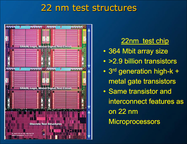
No need to think that with the transition of several factories to 32nm, all of a sudden it will be produced by this technical process - the same chipsets and other peripheral circuits simply do not need it - in most cases they use 45nm. The frontier at 22nm is planned to be fully taken next year, and by 2013 it will most likely be 16nm. At least, this year a test plate (at 22nm) was already made, on which the performance of all the elements necessary for the operation of the processor was demonstrated.
* UPD from nE0 * The need to reduce the thickness of the gate dielectric is dictated by the simple formula of a flat capacitor:
The gate area of the transistor is reduced, and for the transistor to work, the capacitance of the gate dielectric needs to be maintained. Therefore, it was necessary to reduce its thickness, and when it became impossible to find a material with a higher dielectric constant.
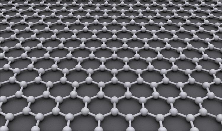
When will the era of silicon end? The exact date is still unknown, but it is definitely not far off. In the 22nm technology, it will still definitely “fight”, most likely it will remain in 16nm ... but then the most interesting things will begin. The periodic table, in principle, is quite large and there is something to choose from) But, most likely, everything will rest not only in chemistry. Increasing the efficiency of the processor can be achieved either by reducing the topological dimensions (they are doing this now), or by using other compounds with higher carrier mobility — perhaps gallium arsenide, possibly “sensational” and promising graphene (by the way, its mobility is hundreds of times higher than that of silicon). But there are problems here. Now technologies are designed for processing plates with a diameter of 300mm - the amount of gallium arsenide needed for such a plate is simply not in nature, and graphene (the Word insistently suggests writing a “decanter”) of this size is still extremely difficult to do - learned to do it, but many defects and problems reproduction, doping, etc.
Most likely, the next step will be the deposition of single-crystal gallium arsenide on silicon, but then already graphene. And, perhaps, the development of microelectronics will go not only along the path of improving technologies, but also along the path of developing fundamentally new logic - this, too, cannot be ruled out. Let's bet, gentlemen? ;)
In general, now there is a struggle for technology and high mobility. But one thing is clear - there is no reason to stop progress.
Tik-Tak
The process of manufacturing processors consists of two large "parts". For the first, you need to have the manufacturing technology itself, and for the second, you need an understanding of WHAT to manufacture and how - the architecture (how the transistors are connected). If both the new architecture and the new technology are made, then in case of failure it will be difficult to find the "guilty" - some will say that the "architects" are to blame, others - that the technologists. In general, to follow this strategy is very short-sighted.
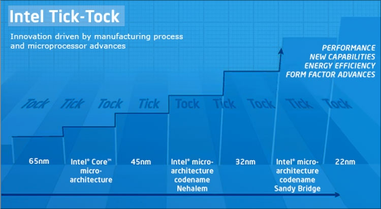
At Intel, the introduction of a new technology and architecture is separated in time - technology is introduced in one year (and the already developed architecture is produced using a new technology - if something goes wrong, technology will be to blame); and when the new technology will be worked out - the architects will make a new architecture for it, and if something does not work on the developed technology, then the architects will be guilty. This strategy was called "Tick-Tack".
| Tick- tock (English tick-tock) is an extensive microprocessor development strategy, announced by Intel at the Intel Developer Forum conference in September 2006. The development cycle is divided into two stages - “tick” and “so”. “Tick” means the miniaturization of the technological process and relatively small improvements in the micro-architecture. “So” means the release of processors with a new micro-architecture, but with the help of the existing technological process. According to the plans of Intel, each part of the cycle should take about a year. |
With the current pace of technology development, fantastic investment in research and development is required - Intel annually invests $ 4-5 billion in this business. Part of the work takes place within the company, but a lot is outside it. It’s almost impossible to just keep the whole lab in the company like Bell Labs (the forge of Nobel laureates).
As a rule, the first ideas are laid in universities - in order for universities to know exactly what it makes sense to work (what technologies are in demand and what will be relevant), all the “semiconductor companies” were united into a consortium. After that, they provide a kind of roadmap - it talks about all the problems that will face the semiconductor industry in the next 3-5-7 years. In theory, any company has the right to literally go to the university and “take advantage” of one or another innovation, but the rights to them, as a rule, remain with the university developer — this approach is called “open innovation.” Intel is not an exception and periodically listens to the ideas of students - after protection, selection at the engineering level and testing in real conditions, the idea has every chance to become a new technology.
Here is a list of research centers around the world with which Intel works (except for universities):
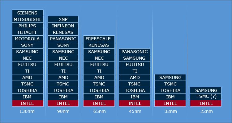
Increased productivity leads to higher prices for factories, and this in turn leads to natural selection. For example, to pay for itself in 4 years, each Intel factory must produce at least 100 working wafers per hour. There are thousands of chips on each plate ... and if you make certain calculations, it will become clear - if Intel did not have 80% of the global processor market, the company simply could not recoup the costs. The conclusion is that owning our own "design" and our own production in our time is quite expensive - at least you need to have a huge market. The result of natural selection can be seen below - as you can see, fewer and fewer companies keep pace with technical progress with their “design” and production. Everyone else had to switch to fabless mode - for example, neither Apple, nor NVIDIA, nor even AMD has its own factories and they have to use the services of other companies.
In addition to Intel, only two companies are potentially ready for 22nm technology worldwide - Samsung and TSMC, which invested more than $ 1 billion in their factories last year. Moreover, TSMC does not have its own design division (only foundry) - in fact, it’s just a high-tech forge that takes orders from other companies and often doesn’t even know what it is forging.
As you can see, natural selection was quite fast - in just 3 years. Two conclusions can be drawn from here. The first is that without your factory the industry leader is unlikely to succeed; the second - in fact, you can succeed without your plant. By and large, there is enough of a good computer, brains and the ability to “draw” - the threshold for entering the market has greatly decreased and it is for this reason that a lot of startups have appeared. Someone comes up with a certain scheme for which there is or is artificially created a certain market - novice manufacturers rise ... PROFIT! But here the threshold to the foundry market has risen strongly and will continue to grow ...
What else has changed in recent years? If you recall, then the year until 2004, the statement “the higher the processor frequency, the better” was quite fair. Since 2004-2005, the frequency of processors has almost ceased to grow, which is associated with access to a kind of physical limitations. Now it is possible to increase productivity at the expense of multi-core - by performing tasks in parallel. But to make a lot of cores on one chip is not a big problem - it is much more difficult to get them to work properly under load. As a result, from this point on, the role of software has cardinally increased and the importance of the “programmer” profession will soon only gain momentum.
In summary, summarizing the above :
- Moore's law continues to operate
- The rising cost of developing new technologies and materials, as well as the costs of maintaining factories are growing
- Productivity is also increasing. A jump is expected when moving to a 450mm plate.
As a result :
- The division of companies into "fabless" and "foundry"
- Outsource major R & D
- Differentiation due to software development
The end
Was it interesting to read? I hope. At least, it was interesting for me to write all this and it was even more interesting to listen to it ... although I also thought at first, "yes, that they will tell in this lecture."
Last week, the second lecture was held at the Moscow Polytechnic Museum, which was held by Intel Fellow, academician Boris Babayan . The lecture was devoted to the history of Russian microprocessor developments - unfortunately, I’ll just not have time to write a similar article on the second lecture. Therefore, for those who could not come, I can only offer this audio lecture.
 [ Download / 180Mb]
This Wednesday (11/24/2010, in the same place) the final lecture of the series “From Sand to Processor” will be held - it will be conducted by Oleg Semenov, head of the Russian Intel Labs. Come, admission is free.
See you soon!
Source: https://habr.com/ru/post/108615/
All Articles